Tool/software:
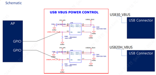
I am trying to apply TPS22963c to a project I am developing. Please review if there is any problem with that part.
This thread has been locked.
If you have a related question, please click the "Ask a related question" button in the top right corner. The newly created question will be automatically linked to this question.
Tool/software:
I am trying to apply TPS22963c to a project I am developing. Please review if there is any problem with that part.
Hi Jaeh Yeon Kim,
The schematic looks good.
Best Regards,
Arush
Thanks for your review.
I have a question about the datasheet.

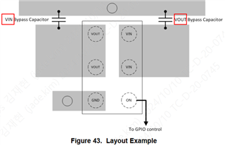
The terms VIN and VOUT are swapped in the picture. Am I understanding this correctly?
Please confirm.
Hi Jaehyeon Kim,
It looks like you are correct. They are swapped. Thank you for pointing this out.
Best Regards,
Arush
I have an additional question.
I purchased TPS22963 and tested it.

SYS_5P0 connected to VIN pin is Off.
Also, ON pin is connected to pull down resistor and is Low.
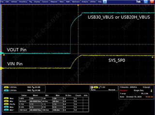
Test is as follows. When connecting VOUT pin to PC via USB cable, voltage flows to VIN pin.
The waveform is the test result.

Why is there voltage flowing through the VIN pin?
TPS22964 has QoD feature. Can I solve this problem by using TPS22964?
Hi jaehyeon kim,
When the EN is low and Vin or Vout >1V, the Reverse current blocking should be active and prevent any current flow from OUT to IN. This is valid for both TPS22964 and TPS22963 devices. QoD won't help here as it looks like USB is forcing 5V at the device out. QoD would have helped if the output was floating/undetermined.
Can you test the device and probe Vin, Vout and EN of the device. Please check if there is any current flow from out to in (if you have access to current probe or SMU). Can you also probe ON pin.
Best Regards,
Arush