This thread has been locked.

If you have a related question, please click the "Ask a related question" button in the top right corner. The newly created question will be automatically linked to this question.

TPS631000: Searching for a bidirectional DCDC SMPS

Part Number: TPS631000
Other Parts Discussed in Thread: TPS55289, TPS552892, INA219, TPS61289

Tool/software:

So i am looking some some other DC DC converter , one that is able to provide 2-3A or more in BOTH directions, i will be operating under 15V, mostly under 5V but i would proffer to be able to use a 12V bus.

Somehow i didnt find much or rather nothing. Somehow all seem to be limited to 0.7A in reverse.

When i did search on the controller side there were 2... and both in huge IC packages.

Is there really no better solution?

Maybe some digital control ( did not search for TI references on this one since i know it can be done )?

THX in advance

  • Hi  Rushing,

    Did you check if TPS55289 is suitable for your case?

    Regards

    Tao

  • I will take a look, it looks promising at first sight.

    I dont really like the idea of I2C for this but not am i against it.

    I wander if there is a fully analogue  IC ? I am currently using a DAC to change the output voltage ( there is some TI reference ).

    Or is there a controller without the 0.7A limitation?

  • Hi Rushing,

    Yes, we have device with FB version, will forward this thread to my colleague to help.

    Hi  Mulin,

    If my remember is correct, we have FB version for TPS55289, right?  Please help to check if this device can meet requirment.

    Regards

    Tao

  • Hi Rushing,

    TPS552892 is the FB version, but it doesn't support bi-directional operation. Can you explain your application? Do you need regulate both Vin and Vout?

    Regards,

    Mulin

  • So here is the setup:

    i have a 12v or 5V DC buss .

    I want to take energy from it and charge  some Li ion cells ( based on some algorithms and measurements done with INA219).

    Then i want to put the energy back in the DC buss with a CC behavior.

    The buss is able to both provide and sink current.

    My aim is to use a single DCDC converter for this task. i know i can do it with 2 identical ones and come extra circuitry.

    Think of it like a power bank, just that we want to also have CC output and input if desired ( there is a MCU that can controls that.

    Do you understand now better?

  • Hi Rushing,

    Thank you for your description, we still have some questions:

    1. How many Li ion cells in series will be? What is the output voltage of the DCDC converter?

    2.What is the input voltage bus from? We have concern that the input voltage will be out of control and causing input voltage out of spec and damage.

    3. Can you show a simple block diagram of your application for us to better understand?

    4.We have TPS61289 for BTS. Please take a look and tell me if it is suitable for your application. https://www.ti.com/product/TPS61289?keyMatch=TPS61289&tisearch=universal_search&usecase=GPN

    Regards,

    Mulin

  • So after some reading it seems to be suitable, but the documentation seems to be lacking here and there.

    So i have a few questions about this IC directly:

    1 can you confirm that the low side is disconnected from high side when the Chip is disabled?

    2 VFB-SET seems to be 0.7 or 0.8V it is not clearly defined or the interval clearly set and i feel confused with Vref_fb that is 1V

    3 COMP pin it is set as input but apparently it can also sink OR source 20uA....?

    4 are there any recommended mosfets for the external one? maybe based on the high voltage rail?

    5  DRV output voltage seems to be 4-6V but there is no information regarding max drive current so no way to calculate R3* gate resistor

    6 I see no clear formula for output in buck or boost modes that takes COMP voltage what reference it is used and output voltage in it

    7 page 12 Figure 7-1. TPS61289 Battery Test System Simplified Schematic  the COMP pin looks to source current , looking at the EVAL board i can clearly see negative voltages are used to sink current from this pin but still not clear formulae

    8 I simply dont understand the EVAL board circuity, or rather the op amp part , i am not sure if they are meant to act as compactors  or (very unlikely) some integrator

    9 Gm block is not explained well, i supose it is this:|| GEA Error amplifier trans conductance VCC = 5.0V 180 μA/V||

    10 if i assumed 9 correctly then there is some current to be pushed in a unknown block and some to be sunk with external circuitry , is this correct?

    11* WHY not simply connect the DACs to the FB pin through a resistor?

    12 Can we use the IC and leave the COMP fin floating? asking since that is a method from another TI appnote

  • Hi Dietrich,

    I will forward this thread to expert for TPS61289 here. 

    Hi Fergus,

    Please hep with this case.

    Regards,

    Mulin

  • Hi Rushing,

    Thanks for reaching out.

    For your questions about TPS61289,

    1. The device has a body diode from input to output side, so, VBUS(VHIGH) voltage cannot flow to Vbat(VLOW), but Vbat can flue to VBUS.

    2&3. VFB_SET is set to be 0.7Vto 0.8V to unsure a saturation of the COMP,

    and COMP pin source 20uA current, this can conduct the diode so that the COMP voltage is clamped with the AMPs output(either current compensation or voltage compensation)

    4. The MOS is chosen with the working voltage and current, usually low Qg is recommended.

    5. The low-side gate driver of the TPS61289 has a 1.5A sourcing current and 2A sinking current capability. Usually choose driving resistor to be 0 is ok.

    6. I'm not sure if you are referring about the relationship between comp voltage and output voltage?

    The comp voltage is used to control the inductor current directly. 

    7. In normal working, the comp pin sources current.

    In EVM, I guess you tested the pin at shut down mode and the output voltage of two amps are negative, which clamps the comp voltage to a negative one.

    Once start working, the current and voltage loop output will rise and the voltage will be a positive one.

    8. In EVM, the two amps works as current compensation and voltage compensation loop respectively.

    The actual comp voltage is chose from the lower one of these two(this is why two diodes are used and comp must to be a source)

    9. Yes. GM block is just a voltage to current error amplifier and has a transconductance gain of 180uA/V.

    In normal boost circuit, it is used to modify a voltage compensation loop with external RC connected.

    10. Right, the GM is the part source and sink current of COMP pin.

    11. FB resistor is designed to regulate the output voltage.

    In our EVM, the GM is designed to be saturation and source a current of 20uA.

    It can be connected to a DAC to release the same function.

    One of the considerations is that, when VBUS rises to a high level, the GM will quit saturation and sourcing current will decrease.

    Furthermore, the sourcing current can change to sink current thus the two diode cannot conduct anymore.

    This prevents the comp from rising stops conduct energy to VBUS and protect the VBUS from over charging.

    12. it is not recommended to leave the comp floating.

    If inner GM is used to regulate the output voltage, a RC is recommended to connect to COMP

    Best Regards,

    Fergus

  • I studied what you wrote but there are still some things that are not clear:

    13 how to chose the COMP resistor and the required opamp output range

    14 IF i sink 10uA from the COMP pin how will that affect my output voltage in buck and boost mode? will it rise? if yes how much relative to the FB network values and potentially COMP resistor

    15 on the eval board there are 20pF and a diode D1 permanently tied to COMP pin are they mandatory?

  • Hi Dietrich,

    Let's discuss the working of a normal boost converter with RC connected to COMP.

    As is mentioned before, the COMP voltage is directly related to inductor current.

    When VHIGH is higher than target(FB>1V)

    the comp sink current and COMP voltage decreases,

    This cause less energy convert from VLOW to VHIGH and causes VHIGH to decrease.

    When balance, Comp neither sink nor source current.

    If the comp is now connected with a diode to amp output, then the diode will clamp the comp from increasing and the voltage will be clamped to the amp output voltage.

    That is the amp controls the converter's current to make a constant current control.

    The main difference is that in normal boost condition, the VHIGH is work as a load (capacitors and resistors),

    In BTS condition, the VHIGH is a const voltage source which can source or sink power.

    As for the three questions.

    1. When the device used as normal boost the RC will be part of the control loop.

    You can refer to other boost converter datasheet for more detail.

    TPS61288 18-V, 15-A, Fully Integrated Synchronous Boost Converter datasheet (Rev. C) (ti.com) 

    9.2.2.5 Loop Stability 

    2.  The comp will not sink current as we want the converter controlled by external current and voltage loop in BTS application.

    This is why FB is set to be 0.7 to 0.8V as the VHIGH bus is fixed

    Only when the VHIGH needs to be controlled like a normal boost, the comp will sink current, this causes the device disconnected from external current and voltage loop.

    3. the 20pF and diode are used as stable and negative voltage clamp for the comp pin.

    The 20pF is always recommended.

    The diode can be neglected when external amp is not used, or the amp has no negative output 

    Last but not least, could you again describe your demands that I can make a rough schematic for you, and we can discuss more?

    Best Regards,

    Fergus

  • THX now i understand

    I will work on a rough schematic with my main ICs and placeholder passives and post it here in a few days.

  • Hi Dietrich,

    Please free to connect me if you have any questions.

    I will wait for your schematic.

    Best Regards,

    Fergus

  • Here my my rough schematic.

    Yes there is no gate driver for the high side FETs since i am still waiting a answer from this:

    https://e2e.ti.com/support/tools/simulation-hardware-system-design-tools-group/sim-hw-system-design/f/simulation-hardware-system-design-tools-forum/1426671/tida-010086-tida-010086-design-guide-differences-vs-schematic

    Here is my ,hopefully last, round of questions :

    16 Do i really need a diode in series with R17? Asking since if i use a very low dropout diode ( on the eval board you used a normal one or at least something with a large voltage drop) i think i can only use positive voltages and buffered DAC ( no external one there is one inside).

    17 How do i size up R17 ? yes i know it should be a few k but how do i calculate /estimate it?

    I know i must draw 20uA or so ( Vcom - Vdrop ) / 25ua ? YES 25uA sine that is my design margin

    18 For R2 is the a max acceptable value ? asking since often SMPS/LDO have a recommendation for the R2 max value.

    Well i will try to select within reasonable values but there is no mention otherwise. Vlow_side will never be over 6V maybe under 5V so is there a minimal current that should flow through the FB network?

    19* My DAC can output HiZ what would happen if i inject current in the COM pin while in buck mode?

    20 Both in Buck and in boost mode am am still not sure how to describe the SW as in:

    We can read the INA219 and get current reading and voltage. lets say we have 1.6A but we need 2A . Lets say DAC is outputting 1.2V atm how should be program the DAC in order to get us to 2A? ( PID later now i must understand the direction of Vdac_out in boost and buck mode)

  • Hi Dietrich,

    For your questions,

    16, for the EVM design, the diode is series with R17 because the comp voltage is chosen from voltage or current loop.

    The two diodes and the sourcing of the comp form a circuit that keep the comp voltage equals to the lower one of the two external loop output.

    In your case, the comp is connected to a DAC thus diode is not needed, and COMP pin would be better to sink current.

    Please ensure the output current of the DAC is higher than the sinking current of COMP pin 20uA.

    As a result, the FB voltage should be set to be higher than the setting point 1V.

    In a word, the comp voltage is the one to control, which direct control the inductor current.

    17. R17 and C31 is designed to form a filter to keep the comp stable. Usually, its bandwidth within switching frequency will be helpful.

    18, for R2, it is designed to keep its current 100 times higher than the leakage of the FB pin, then we can calculate the max R2 is 200k.

    Vlow_side will never be over 6V maybe under 5V so is there a minimal current that should flow through the FB network?

    This related to VHIGH side not VLOW side, I guess it could be a clerical error.

    19, When the ADC is HiZ, the comp is regulated by itself.

    When in boost mode, the device will try to regulate the VHIGH voltage.

    Here we have two situations.

    If VIGH net can be regulated, like connect to a resistor, or a load.

    This will be much like a normal boost converter. 

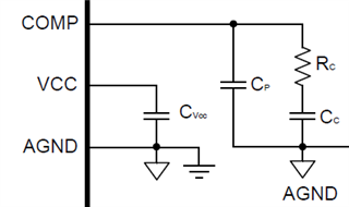
    It is recommended to use such circuit below:

    This forms a compensation network which will help the boost converter to keep stable.

    Another situation is that VHIGH is unable to regulate (like a BUS able to source or sink enough power),

    the comp voltage will be clamped to its max or minimum value, and the device keeps charging or discharging with its max capability 

    When in buck mode, the VHIGH is impossible to be regulated and the comp will keep sourcing or sinking current with its max value(depend on the VHIGH voltage),

    The comp voltage will be clamped to its max or minimum value, and device keeps charging or discharging with its max capability.

    In a word, the device will always try its best to regulate the VHIGH voltage.

    20. As is said before, the comp voltage directly controls the inductor current.

    For example, the DAC is 1.2V, and Comp is also 0.7V(be clamped by DAC), current is 1.6A.

    If 2A is wanted, then DAC value should be higher. 

    Then we change DAC to 1.4V, and current rises to 2.5A, we know we should decrease the DAC.

     Here current feedback is recommended to regulate the DAC and to gain a desired current.

    The buck and boost mode both control the abs value of the current, so the logic is the same in both modes. (comp rises, current rises)

    Be care that the current direction changes and causes the current sense different in two modes.

    Another need to mention, the Drain of Q25 should be connected to SW pin of the device.

    Please feel free to ask if you have more questions.

    Best Regards,

    Fergus

  • THX

    Yea mistakes were made since it was a fast draft so that we can get going with the IC and decide actual system requirements and other system needs.

    BTW since Vcopm pin is between 0.6 and 1.6V then setting the DAC voltage reference to 2V or close will be more then enough ?

    Also the middle of the voltage range is about 1-1.1V supposedly if we cant get the DAC to start HiZ is this DAC value ok as a starting point? ( through probably 5-10k resistor probably)

  • Hi Dietrich,

    If you are not using feedback of the current sense at starting,

    it is recommended to start at COMP voltage of 0.8V

    the relationship between comp voltage and inductor current are almost linear.

    0.8V means a current below 2A.

    The device's current is 20A with comp=1.6V and it looks too large for your application.

    It is highly recommended to use current feedback (either analog or digital compensation) to regulate the current at any time to keep the current control stable and accuracy.

    Best Regards,

    Fergus

  • I will focus on the design for now and later when i am done ill maybe start another topic for a potential review

    THX again for all the help

  • Hi Dietrich,

    Always welcomed to share your design to us.

    Best Regards,

    Fergus