This thread has been locked.

If you have a related question, please click the "Ask a related question" button in the top right corner. The newly created question will be automatically linked to this question.

UCC28730: UCC28730 Buck converter

Part Number: UCC28730
Other Parts Discussed in Thread: PMP22557

Tool/software:

Hi,

I am trying to make an ultra low quiescent current buck converter. I saw your PMP22557 reference design after designing it myself, and found it quite similar.

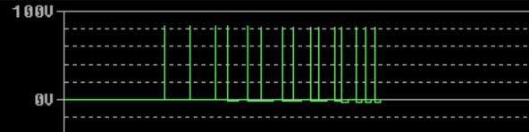
However, there are some oddities. I noticed that the test report shows a significantly higher quiescent current than expected. Some of this is clearly due to the 10k pull down resistor, but that does not cover it all, only about half.

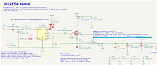
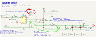
I am wondering if the issue is because of the reverse bias of the HV pin when it is in the MOS ON state (see red arrow "i" in drawing below). Since it is a floating GND connection, with some 8-28V on the VDD pin, the HV pin will be in reverse bias.

Can you confirm? (could you also critique whether my design is wrong in some way...)

  • Some of the inductor comments are a bit off; I tried a whole load of different inductor resistor combinations before settling on the 68uH, and the comments did not really keep up...

    The 12V rail I also decided shall be 15V instead, since what I really want is a stable 5V, so allowing it 3V extra sag room and using a secondary DCDC rated beyond 15V seemed sensible.

    It must be able to sustain a ~250mA load step from  near zero to running on the 5V for at least 30ms for worst case recovery. If it can achieve that I am happy.

  • I am thinking I should add this diode to protect the HV pin from discharging the cap. Thoughts?

  • Hi David,

    Thank you for reaching out.

    The 10k resistor is a preload resistor and it is generally used in PSR controllers to maintain regulation at light loads.

    I am not able to see the startup resistor Rvs1 in your schematic. Ivsl(rrun) current is injected here to startup the system at desired voltage.

    Ideally HV can be directly connected to Vbus to provide the required startup current to charge Vdd cap after which the internal JFET turns off and the Vdd is supplied from output side.

    Other than this the schematic looks fine.

    Regards,

    Harish

  • Hi Harish,

    Thanks for the response.

    Can you explain more about Rvs1 and Ivsl(rrun)? Is this related to R8 R9 and D2 in the PMP22557 schematic? I am slightly lost. I understand that current out of the Vs pin determines the bus voltage measured by the chip, I have 180kohm wthich will pull (Vbus-Vout)/180k.. typically 250uA-1mA at the 40V to 160V I plan to run it. Note that the wire is connected by a net label "VS". Am I missing something?

    Also could you address the reverse bias? I presume from your explanation that the 700V JFET is blocking in both directions when off and so resists current flow out of the device, negating the diode I added? and in the transition period where it is charging through the JFET but has started switching and the output is not sufficient to bootstrap it?

    Thanks

    David

  • Hi David,

    The path for the current from Vs pin to turn on the converter at the required voltage will be Ivsl(run) x (R1+R8+R9) as shown below:

    The regulation of output voltage will be done through R1 and R2.

    Regarding the diode, most of our designs do not need this diode on the HV pin. If the output voltage is not up to take over during the transition period, the aux winding will still not not be up and the IC will attempt restart until the time when IC establishes output voltage.

    Regards,

    Harish

  • Do I need the D2 per your marked up diagram for my design to work? I currently have the same path, but with the 150k, and 2x15k resistors combined to one 180k...D1 confuses me a bit as well in your diagram. 1n4148 is a 100V rated part, but your DCDC is for up to 160V and I think D1 sees 160V*150/(150+15+15) = 133V (albeit with current limited due to the 2x15k resistors)

    Thanks

    David

  • Hi David,

    I think both the schematics are different. The reason being, the voltage sense path is decoupled from the startup path with the usage of diode D2. So startup resistor will be determined by R1, R8 and R9 whereas the regulation resistor is determined by only R1 and R2 in the schematic I posted.

    D1 is a low voltage diode connected to Vdd less than 100V. Please refer below simulation.

    I recommend you download PSPICE model to create this buck stage to verify this.

    Regards,

    Harish