


Other Parts Discussed in Thread: TPS84250,
Tool/software:
Hello.
It contains 4x TPS84250 and 4x TPS84259.
The four TPS84250 outputs are set to +11.5V, because I connected a 133K 0.1% resistor between VOUT and VADJ, which is the pin 36.
The four TPS84259 outputs are set to -11.5V, because I connected a 133K 0.1% resistor between VOUT and VADJ, which is the pin 36.
For all cases the input voltage is +24V, and there is a schottky diode from this +24V to the input of each chip.
I created this topic looking for a review of layout of the TPS84259. There is four power supplies using it, I did the layout of it one time, and I would like to validate it, then later I will do a copy for the other three.
To say, my layout for the TPS84250 was "approved" by an engineer of Texas Instruments, and the link for this topic is below.
e2e.ti.com/.../tps84250-layout-review
The simplified stack of the PCB, only considering the copper layers, is:
L1: Top
L2: Ground plane
L3: Power plane. Multiple +11.5V planes
L4: Power plane. Multiple -11.5V planes
L5: Ground plane
L6: Signals + ground
L7: Ground plane
L8: Bottom
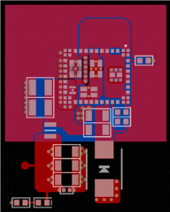
Below are pictures of my layout with the TPS84259, to be validated. Below is not shown how is L6, but in L6 at the chip area there will be a ground fill, similar to L8, bottom, but enlarged.
General view:
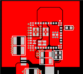
L1, Top:
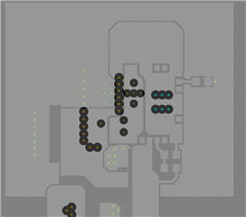
L2 and L5 and L7, Ground planes:
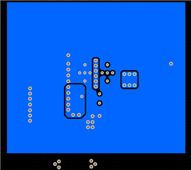
L8, Bottom:
Does my layout looks fine?
Regards.
