Other Parts Discussed in Thread: AM2431, TPS22965, TPS54320
Tool/software:
I have some questions about PMIC timing. PMIC part number is TPS6521908, MPU is AM2431.
Please assist in analyzing the causes and assessing the risks.
Thank you.
1.Power On Sequencing Issue
The sequencing between Buck1 0.85V and MCU OSC0-XO is reversed, We don’t know why it happened. What effect will the reversed timing cause?
Test point is MCU OSC0 XO output pin.
|
Item |
Measured Value |
|||
|
Time between Buck1 0.85V and MCU OSC0 XI/XO |
-3ms |
3ms |
||
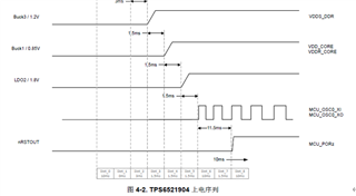
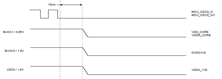
The test waveform is as follows, and required timing sequence is used for comparison.

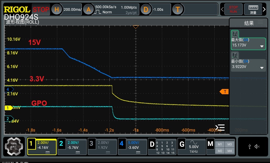
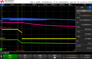
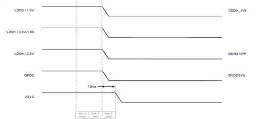
2.Power Down Sequencing Issue
1)The sequencing between Buck1 0.85V and MCU OSC0-XO is reversed, We don’t know why it happened. What effect will the reversed timing cause?
Test point of MCU XI/XO is MCU OSC0 XO output pin.
2)The sequencing between GPO2 and VSYS is reversed, We don’t know why it happened. What effect will the reversed timing cause?
Test point of VSYS is PMIC Power input 6/20/22 pin.
|
Item |
Measured Value |
|
|
Time between NRSTOUT and Buck3 1.1V |
0.16ms |
>=0ms |
|
Time between Buck3 1.1V and MCU XI/XO |
8.5ms |
0ms |
|
Time between MCU XI/XO and Buck1 0.85V |
-8.4ms |
10ms |
|
Time between Buck1 0.85V and Buck2 1.8V |
0 |
>=0ms |
|
Time between Buck2 1.8V and LDO3 1.8V |
0 |
>=0ms |
|
Time between LDO3 1.8V and GPO2 |
0.04ms |
>=0ms |
|
Time between GPO2 and VSYS |
-1.1ms |
10ms |
The test waveform is as follows, and required timing sequence is used for comparison.


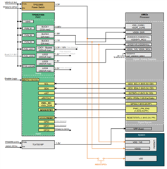
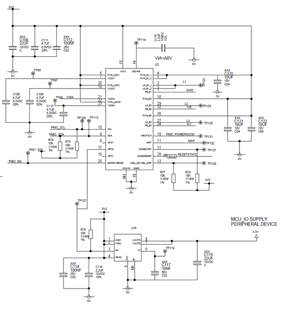
Here is the schematic diagram of PMIC section as below. Please help check. Thank you.

Thanks.