Tool/software:
Hi Expert,
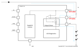
Tps92611-Q1 happens fault. The the resistor between between Supply and GND is 18.6 oHm, the resistor between IN to GND is 179 oHm. Can you give some reasons seeking directions?
This thread has been locked.
If you have a related question, please click the "Ask a related question" button in the top right corner. The newly created question will be automatically linked to this question.
Tool/software:
Hi Expert,
Tps92611-Q1 happens fault. The the resistor between between Supply and GND is 18.6 oHm, the resistor between IN to GND is 179 oHm. Can you give some reasons seeking directions?

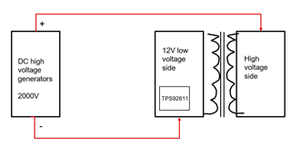
Add information: The tps92611 PCB is placed in a Metal box, the injection voltage is DC 2500V. You can see the reference diagram as figure.
Customer wants to know, based on the resistor of SUPPLY and IN, the DC high path is Out-->IN or IN-->OUT?
Hi Beida,
Can you provide some information on the fault condition? What exactly is the problem that you are seeing? What is the voltage you are measuring at the SUPPLY and IN pins? What is the voltage measured at the OUT pin? Are you using PWM dimming?
The the resistor between between Supply and GND is 18.6 oHm, the resistor between IN to GND is 179 oHm.
Can you confirm the resistance of the sense resistor shown in your diagram? I'm not sure why you are measuring resistance from the pins to ground, the sense resistor is between the SUPPLY and IN pins. If the sense resistor is 18.6 Ω, the device is configured for an output current of 5.2mA. Is this your desired output current?
Customer wants to know, based on the resistor of SUPPLY and IN, the DC high path is Out-->IN or IN-->OUT?
I believe you are asking about the direction of the output current? Linear LED drivers are configured for current to flow in a single direction, depending on if it is a current source or a current sink. The TPS92611-Q1 is a current source. During normal operation the current can only flow in the direction of the blue arrow you drew in your diagram.
Regards,
Zach
Hi Zach,
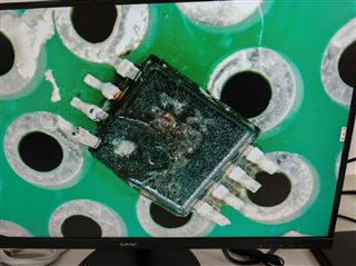
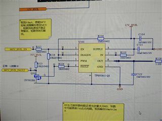
Pls see the fault device and schematic. Today customer found another failure device. After remove device from the PCB, customer measure that the resistor of OUT pin to GND is 9.6 oHm. While Supply pin to GND is 16.2 Ohm, the IN to GND is 16.7oHm. The release path of the high pressure is from the IN pin to GND or OUT pin to GND?
Hi Beida,
From your image, it looks like there is visible damage at the supply pin. I suspect there is some overvoltage condition due to your 2500V at the high side of the transformer.
Is this meant to be an isolated supply? If so, your diagram is incorrect. The low-side ground should be isolated on the other side of the transformer winding and should not be shared with the high-side ground. See diagram below. If the board is configured as shown in your previous diagram, I would expect components to be damaged.

I am also not sure why you are referring to a DC injection voltage. The voltage must have an AC component for the transformer windings. You should also have a rectifier circuit on the low-side. Can you confirm which transformer diagram shows the correct connections? Are you able to provide a schematic of your entire system including the connections between high and low voltage?
Regards,
Zach
Hi Zack,
The tps92611 PCB is placed in a Metal box, the high voltage is connected to GND of box. While the gnd of TPS92611 is also connected to box. The DC 2500V is Instantaneous injection, which is to pass the production compliance withstand test. Can you understand the application condition?
The problem focus: When the high voltage is flowing through TPS92611 and cause the device broken. Based on the Supply pin to GND is 16.2 Ohm, the IN to GND is 16.7oHm, OUT pin to GND is 9.6 oHm, which pin is the possible high voltage input port?
Hi Beida,
Please provide the detailed schematic of your TPS92611-Q1 board and test configuration including external connections.
Please refer to Table 6.1 in TPS92611-Q1 datasheet. These are the absolute maximum ratings of the device. If your high voltage injection causes the voltage at the pins to exceed their absolute maximum rating the device will be damaged.
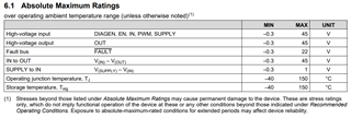
Regards,
Zach
Hi Zach,
The schematic of customer is NDA. Can you provide me the Failure Tree of TPS921611? We want to locate the root cause.
You can send me by email. Thanks.
Hi Beida,
Are you looking for the failure mode distribution? I should be able to provide this, as well as the FIT rate. However, this event seems to be due to an overvoltage condition that violates the absolute maximum ratings of the device, whereas the FIT rate is a measure of reliability in standard operating conditions.
Again, please note that violating the absolute maximum voltage ratings will cause failures.
Can you provide your email address? For some reason I am unable to look up your profile on E2E. You may send me a private message on E2E if you do not want private information on the forum.
Can you also provide any information on your test procedure? Is there a particular standard you are testing to? What is the specific name of this type of test?
Regards,
Zach