This thread has been locked.

If you have a related question, please click the "Ask a related question" button in the top right corner. The newly created question will be automatically linked to this question.

LM3488: Unable to switch. DR pin is constantly ON.

Part Number: LM3488
Other Parts Discussed in Thread: LM3478

Tool/software:

Hi,

I am experiencing some issues where the boost converter doesn't switch. Please see my attached schematic (VR1 is set to 10K). My Vin is set at 4V, and my output is loaded with a 1k ohm resistor. For some reason, DR always matches V_IN voltage, but my voltage at TP7 is close to V_IN.

I read from other posts that a potential high inrush current could lock up the controller, but I didn't notice any spike in voltage from the input, output, or I_SEN. Were any potential mistake(s) made with this schematic? Thanks.

  • Hello Kenneth,

    Thanks for using the e2e forum.
    I do not directly see any wrong connections within the schematic. You can use our quickstart calculator tool to double check the compensation and inductor selection:
    https://www.ti.com/tool/download/LM3478-88-BOOST-CALC

    A question on the failure description:
    If Vout is following Vin, it would suggest that the device is not switching, DR pin stays at 0V and the IC is not operating.
    You mentioned that DR voltages matches Vin voltage. Is this the voltage you measure at TP5?
    The DR voltage should stay in the range of 0V - 7V VCC voltage. If you see Vin voltage on the DR signal, the IC might be damaged.
    Can you confirm if the driver is not switching at all (also during startup)? And if it switches, please double check the voltage level of DR.

    Thanks and best regards,
    Niklas

  • Hi Niklas,

    Thank you for your reply and for sharing the tools. It is very helpful.

    I used the quickstart tool and changed my Rcomp, Ccomp, and CHF. I could now see the DR switch, but it's rather odd. The following are snapshots of the captured signal (Yellow = DR, Green = output, Blue = Vin, and Red = feedback). My PSU input was set to 4V, and the circuit is drawing a relatively high amp at close to 0.25A without any visible boosting). My MOSFET (SIR610DP-T1-RE3) has a Vgsth of 2V to 3.6V. It seems like the MOSFET was unable to be switched on. Do you think that is a possibility? 


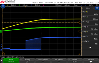
      (Zoomed-in view of the DR switching)
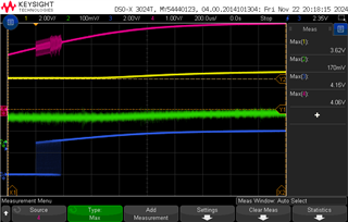
  • Hi Kenneth,

    If you are working with 4V input voltage, I would recommend to try a logic level MOSFET, which have their  Vgs threshold between 1V and 2V.
    If the application is still not working, we need to look deeper into the design once more.

    Best regards,
    Niklas

  • Hi Niklas,

    Apologies for the delayed response. I adjusted the input voltage to 7V to test the circuit. It seems the MOSFET is turning on, as it was heating up when observed through my thermal camera after the DRV pin went high. I also noticed that the DRV pin is now switching longer before locking up. I also set the FA resistor to 400 kHz, but this did not improve the output—the circuit isn’t boosting. Do you have any suggestions on what else I could check? Thanks!

    Yellow = output

    Green = FB

    Blue = DR

  • Hi Kenneth,

    Thanks for the update.
    What makes no sense to me is that the blue signal is stated to be the DR pin (TP5) and not the switch node pin (TP7).
    If the drive pin goes high 100%, the inductor should saturate, leading to an input short that likely destroys the MOSFET due to overcurrent.
    I do not see any drop of the Vin voltage and also no triggering of the overcurrent protection of the device, which should pull down the driver signal.

    Aside from this, I looked further into the MOSFET and diode component.
    The Vds rating is 200V. Based on your feedback settings, the output target voltage is ~32V, so a 60V rated MOSFET would be fully sufficient here and could improve efficiency.
    Same goes for the schottky diode which has the same 200V rating.

    Could you also share the specs for the 4.5uH inductor?
    Right now you are only using 1kOhm resistor for the load. Will this also be the expected peak load, or will this be higher in the final applicaiton?

    Best regards,
    Niklas

  • Hi Niklas,

    Thank you for your feedback. To clarify, the yellow trace represents TP7.

    I completely agree with your thoughts. This is why I initially suspected the MOSFET was not turning off, as I did not observe a short when DR was consistently high. That said, I will double-check the labeling on the plot since I obtained this information from my test engineer.

    Our target is to achieve 100V output, but since this circuit is readily available in our lab, we decided to test how much higher we could push the output with it. This also explains the choice of a 200V-rated MOSFET and diode. Efficiency isn't a critical factor here, as the circuit is only intended to operate for a very short duration.

    For the inductor, we used the Bourns SRR1208-4R5ML. Eventually, this setup will be used to drive a piezoelectric transducer with high-side and low-side switching through a two-phase three-wire transformer, so the load characteristics will not be static. 

    If you have any recommendations for improvement (like a better chip), they would be greatly appreciated! That said, we are also keen to uncover the root cause of why this circuit didn’t function as expected. Solving this mystery will provide valuable insights for our future designs.

    Thank you.

    Kenneth

  • Hi Kenneth,

    Thanks for the quick answer and double checking the waveforms.

    If Vout target is 100V, that the ratings make more sense. Then the bottleneck will be the low input voltage.
    A pure boost topology normally gets to its limits at a boost factor of 8 or 9 times the input voltage, simply because the off-times of the MOSFET become so small, that not enough power can be transferred to the output side. For Vin 4V, an output voltage of 32V is already close to the limit.
    Our other Boost controllers also list a maximum duty cycle in their datasheet, which is normally around 90% to 96%.

    The LM3488 lists a maximum on time of 100%. This comes from the fact that this device is based of a Buck controller originally, where 100% mode just means bypass. In Boost topology, 100% mode would be an input short, so there are still the same boost factor restrictions that apply here.

    If higher boost ratios are required, we recommend a flyback topology instead. The different winding ratios then allow for higher boost ratios with the same duty cycle.

    Best regards,
    Niklas

  • Hi Niklas,

    Thank you. We will look into flyback topology next. In the meantime, do you think there's anything left to troubleshoot for our design? We still cannot figure out why it doesn't switch.

    We did another round of probing, and this is the result. Rather than using names, I will refer them to the TP in my schematic. I hope you were able to find out what went wrong. Thanks!

    Yellow = TP8

    Green = TP6

    Blue = TP5

    Red = TP7

  • Hi Kenneth,

    Thanks for the update and considering flyback topology.

    My strongest suspicion is still about the SIR610DP-T1-RE3 MOSFET which is used.
    If possible, I would recommend to test a different MOSFET with lower gs-threshold.

    You can also request a free sample of our LM3478 Boost EVM for further testing. (The LM3488 is pin2pin with the LM3488)
    https://www.ti.com/tool/LM3478EVAL

    Best regards,
    Niklas