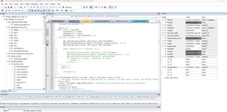
This thread has been locked.

If you have a related question, please click the "Ask a related question" button in the top right corner. The newly created question will be automatically linked to this question.

BQ76952: Question about BQ76952

Part Number: BQ76952


Tool/software:

Hello:

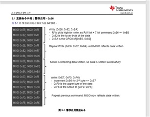
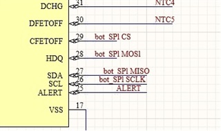
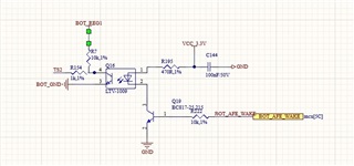
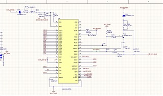
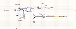
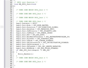
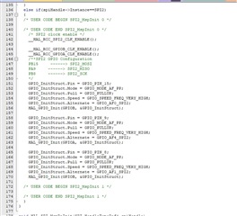
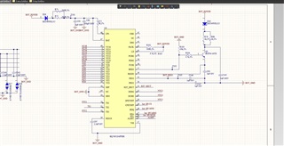
This is the recommended circuit diagram for the TI chip BQ7695204PFBR used by the customer. Currently, SPI communication is being used, but the data returned is consistently incorrect. Communication cannot be established, and it keeps replying with the data 0xFFFFFF. Whether writing direct commands or subcommands, there is no data.

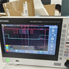
I feel like the waveform is fine too

The data returned is always 0xFFFFFF. If you know the situation, please let me know

  • Hello Jimmy,

    For subcommands, we usually recommend adding at least a 2 ms wait time to give enough time for the subcommand to complete operation. It is weird that this is occurring with direct commands as well.

    Do you mind sharing a logic analyzer file and your configuration file (.gg) as well? I’ll review those with your schematic to get a better picture. Also, what commands were you trying to send?

    Best Regards,
    Alexis

  • Hello Alexis:

    The waveform captured by the oscilloscope in the following figure is the same as that of the logic analyzer. In addition, the customer tested SPI communication using SPI loopback mode, which can transmit data。

    1、Now I suspect that the TI chip needs to wake up pin TS2 every time it is used before it can be used?

    2、Also, may I ask if the default communication of BQ7695204 chip is verified by SPI communication and CRC8?

    3、Also, the customer is currently providing a series resistor to simulate the voltage of the battery cells, with each voltage being 1.5V. Is it possible that the battery cell voltage is too low, causing it to sleep when powered on? thank you


  • Hello Jimmy,

    1. If the device is in SHUTDOWN mode, you would need to wake up the device with the TS2 pin before being able to communicate with it.

    2. SPI communication has an optional 8-bit CRC check. The interface must use 16-bit transactions if CRC is not enabled and must use 24-bit transactions when CRC is enabled. This is further discussed in Section 9.3 SPI Communications Interface in the BQ76952 Technical Reference Manual (TRM). The Software Development Guide there is showing an image of using SPI with CRC. 

    3. SLEEP mode is dependent on the current, so it is entered when there is low current detected. Your voltages should be fine to simulate cell simulators. Section 13 Device Functional Modes in the BQ76952 Datasheet helps show the different modes how it’s entered/exited. Section 7.3 SLEEP Mode in the TRM describes more about SLEEP mode.

    Can you please still send us the logic analyzer files?

    Best Regards,
    Alexis

  • Hello Alexis:

    1. This device should be awakened because REG18 has already output 1.8V. In addition, BOT-REG1 has output 3.3V and TS2 is at a low level, so it feels like the device has been awakened. LD is directly connected to POWER,

    2. Does BQ7695204 default to SPI communication for this issue? Will the reset and SHUTDOWN modes automatically switch to IIC communication? Or will it automatically revert back to SPI mode after resetting and shutting down?

    3. Is CFETOFF the default chip selection signal for this chip? Is HDQ the default MOSI signal? Does SDA default to MISO and SCL default to SCLK? Do these multiplexed pins need to be configured before they can be used.

    4. Can you confirm that there are no issues with the connection of our hardware circuit diagram.

    5. Can you confirm whether there is a hardware problem or a software problem.

    6. Can you provide me with an SPI communication program specifically designed for this chip? The routine downloaded from the official website is not specific to this chip.

    7. Are there any configuration errors in the initialization of the program? The phase and baud rate should not be configured incorrectly, right.

    8.We don't have a logic analyzer yet. Let's buy one later to test it and see if the clock it returns is 0xFFFFFF.

    9. Can you confirm that the BQ7695204 chip must have SPI communication, whether it is initialization, reset, or SHUTDOWN? Finally, can you confirm whether there is a hardware problem or a software problem.

    10. Is there a detection method that can determine whether the device is in normal mode and can communicate normally, or in sleep or SHUTDOWN mode, by detecting the voltage on the pins of the device.

    11.We don't have the waveform of the logic analysis instrument yet, we are buying it. Also, if the CS signal of the device is not selected, will it keep returning 0xFFFFFF

  • Hello Jimmy,

    1. Can you check the 0x12 Battery Status()[SLEEP] bit to confirm if the device is in SLEEP mode or not?
    There is also a chance the device has entered Soft Shutdown state especially if the SHUTDOWN sequence is initiated and the TS2 pin remains LOW or the LD pin remains HIGH. This Soft SHUTDOWN FAQ and SHUTDOWN Mode FAQ may be useful it that’s the case.

    2. For your device version, BQ7695204, the default communications interface is SPI as shown in Section 5 Device Comparison Table of the BQ76952 Datasheet. The reset and SHUTDOWN mode should not switch the device to I2C communication because of that unless you OTP the part to do so otherwise or manually switch it yourself.

    3. For the BQ7695204 version, the CFETOFF and HDQ should also default to SPI CS and SPI MOSI.

    4. Your hardware circuit diagram seems to be fine overall. Some things to point out: a) The TS2 pin doesn’t really need the external connection to REG1 as when the part is OFF, REG1 will also be OFF. b) The LD and PACK pin resistors seem small. Smaller values will make the pins weaker to ESD. We usually recommend ~10kOhm resistors.

    5. This could be more of a software problem from the looks of it. As mentioned in the TRM and datasheet, 'If the host performs a write with CRC and the CRC is not correct, the incoming data is not transferred to the incoming buffer, and the outgoing buffer (used for next transaction) is also reset to 0xFFFF.’ Another possibility is the internal oscillator of the device may not be running when the host initiates a transaction. This can occur if the device is in SLEEP mode and will cause the interface of SPI_MISO to drive out 0xFFFF for the first 16-bits clocked out. Further information regarding this can be found in Section 14.3.1 SPI Protocol in the Datasheet and Section 9.3 SPI Communications Interface in the TRM.

    6. I’m not quite sure what you mean by this question. Section 5 SPI With CRC Examples in the BQ769x2 Software Development Guide provides examples of using SPI with CRC correctly and the previously mentioned sections in the TRM and datasheet should provide more information regarding the protocol and interface.

    7. There shouldn’t be any configuration errors in the initialization of the program unless the user has changed somethings incorrectly.

    8. Please do. This can help provide us more information on if communications have been done correctly.

    9. This has been answered above.

    10. If the device is in SHUTDOWN mode, the REG18 pin will output 0V, otherwise REG18 LDO will output 1.8V. As mentioned above, 0x12 Battery Status()[SLEEP] bit will tell you if the device is presently in SLEEP mode or not.

    11. Can you explain what you mean by the CS signal of the device is not selected?

    Best Regards,
    Alexis