This thread has been locked.

If you have a related question, please click the "Ask a related question" button in the top right corner. The newly created question will be automatically linked to this question.

LM5156: Pulse Skipping implementation details

Part Number: LM5156
Other Parts Discussed in Thread: LM5155, , TPS61175

Tool/software:

Hi,

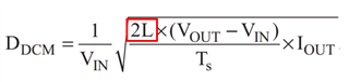
I find that the Datasheet for the LM5156 does not define clearly how pulse skipping is implemented. Other related forum questions seem to suggest that the implementation is similar to other IC families such as LM5155 and APT61776 etc.

I have found Application Report SLVA353 - July 2009. This describes such a pulse skipping mechanism in some detail. Does the LM5156 use the same technique?

Thanks in advance

Aidan

  • Hi Aidan,

    The pulse skipping is related to the minimum on-time capability of the device.
    In light load condition, the device will try to keep a consistance PWM signal with fixed frequency for as long as possible, but if the duty cycle would become so small, that the required on-time of the MOSFET would be smaller than the on-time restriction of the device, it will start pulse skipping to avoid a runaway of the output voltage.

    The entrance point of the pulse skipping mode can be adjusted by the inductance. A larger inductance will increase the duty cycle in DCM operation and therefore increase the on-time of the device.

    For LM5156, the minimum on-time capability follows the switching frequency. Therefore changing fsw will not affect the pulse skip behavior of the device.

    Please let me know if additional question come up on this.

    Best regards,
    Niklas

  • Hi Niklas,

    Actually this was very useful thanks for pointing out the graph, it was not actually referenced in the datasheet text description and it was not therefore clear that this relationship exists. It is quite important in particular with regard to peak currents. It would be helpful if you could clarify the exact mechanism by which this gets implemented in the IC. If I understand this correctly and I would appreciate your confirmation; the min-on-time is frequency dependent as you have stated, and during a gate on period, this min-on-time will be honoured regardless of the state of the PWM reset trigger, or in fact the current limit reset trigger? In this way if for example we have a very large leading edge spike or we have an undersized or saturated inductor it is quite possible to have very large currents flowing in the FET during this short period.

    Can you confirm if the LM5156 uses the same internal logic as that described in the application note that I originally referenced in order to generate the pulse skipping process and can you also confirm as it is not clear even in the application note, if the current limit reset trigger is ignored during the minimum-on-time. That is to say once the gate pin has been driven high, it will stay high for the min-on-time regardless of whatever other signals are evident in the system, including the current limit comparator?

    Looking forward to further feedback.

    All the best

    Aidan

  • Hi Aidan,

    the min-on-time is frequency dependent as you have stated, and during a gate on period, this min-on-time will be honoured regardless of the state of the PWM reset trigger, or in fact the current limit reset trigger?

    Yes, this is correct. Even if overcurrent protection would be triggered during the minimum on-time period, the driver voltage would still stay high until minimum on-time is fulfilled and then shut down.
    There is also an additional blanking time at the beginning of every cycle where the OCP cannot be triggered. This is exactly to filter inrush current due to the turn-on of the FET.

    Reading through the app note you reference, I am not fully sure if the implementation is identical to LM5156, as I do not know the TPS61175 device.
    For LM5156, the mechanism also includes the voltage at FB. The device switches with minimum on-time until Vout rises to the OVP threshold. Then the device will stop operation (enter pulse skip mode) and only sends out pulses if FB drop.

    Best regards,
    Niklas

  • Except if used in Flyback when FB is grounded Slight smile

    Do you know the leading edge blanking time?

    Thanks

    Aidan

  • In fact my earlier question about how exactly the IC detects that FB is grounded I feel was not answered very effectively. As you are being so helpful I would like to try again. The datasheet says that when FB is grounded 'flyback' the COMP min voltage clamp is disabled. How does the IC know that FB is grounded if it does not seem to measure it somehow?

    LM5156: Detection of FB pin tied to GND for flyback mode - Power management forum - Power management - TI E2E support forums

    Any more insight?

    Thx for everything

    Aidan

  • I will take a stab at this answer myself and tell me if you agree. The only source of current onto the COMP pin internally to the IC is the error amplifier. When FB is grounded as soon as SS begins to rise the error amp will always try and drive the maximum sourcing current of 180uA onto the COMP pin and it will, unless otherwise pulled down for example by am optocoupler, rise towards its maximum 2.85V. 

    Why then is the COMP pin pulled up to VCC by an external resistor in flyback configuration.

    Aidan

  • Hi Aidan,

    Thanks for the feedback.
    The blanking time is ~50ns.

    In Flyback topology with FB connected to ground, the skip mode mechanism does not work.
    The duty cycle is defined via the COMP pin regulation. However, even if COMP goes down to 0V, the device would keep operation with minimum duty cycle. This is because FB can never trigger overvoltage as it is connected to ground. Hence, the device does not stop switching.

    Therefore is is recommended to place a clamping diode on Vout in flyback topology to avoid Vout runaway in zero load conditions.

    Best regards,
    Niklas