This thread has been locked.

If you have a related question, please click the "Ask a related question" button in the top right corner. The newly created question will be automatically linked to this question.

TPS6594-Q1: The PMIC's SOC_RAIL_TRIG selects MCU power error, nPWRON/ENABLE=1, BUCK5 has no output power, and no interruption event occurs.

Part Number: TPS6594-Q1
Other Parts Discussed in Thread: TDA4VL

Tool/software:

Hello,

The PMIC we used is TPS6594133ARWERQ1, SoC is TDA4AL or TDA4VL, and the power supply scheme we use is the J784S4 PDN-3F.

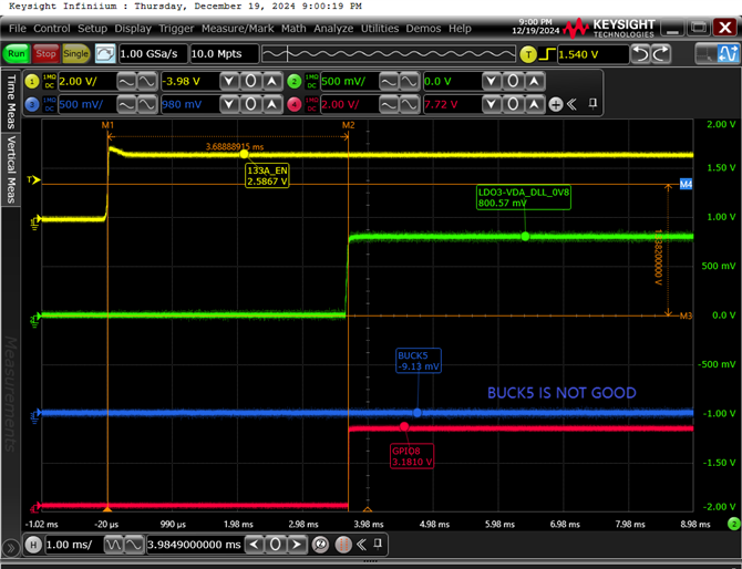
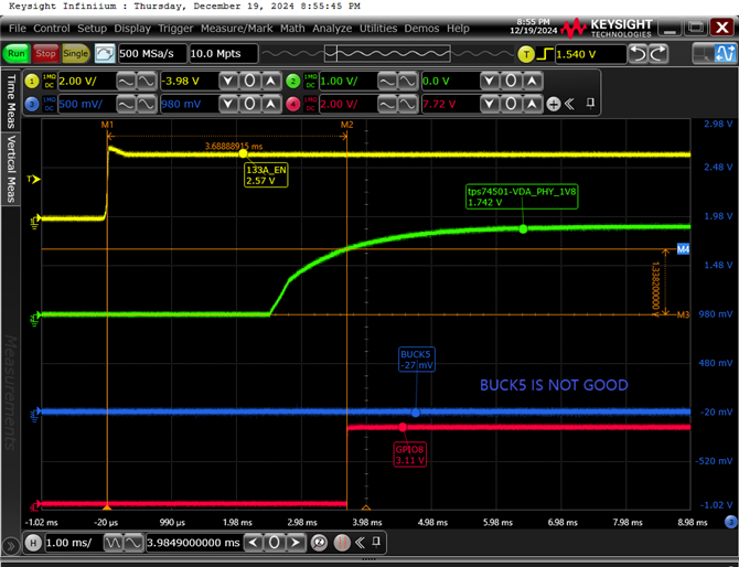
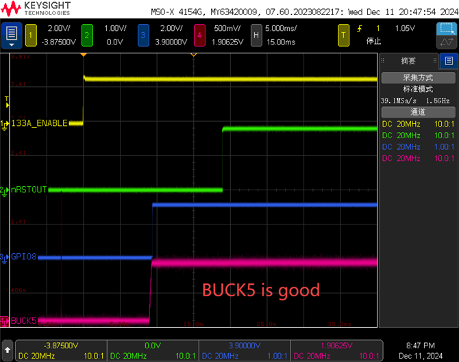
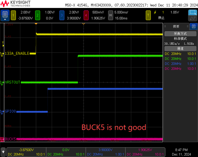
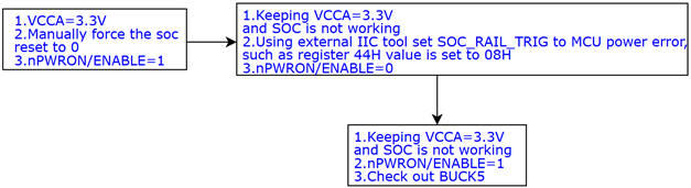
At present, we find that as long as SOC_RAIL_TRIG is configured as MCU power error when nPWRON/ENABLE=1, and then the PMIC is re-enabled(VCCA maintains power supply), BUCK5 will appear without output power.

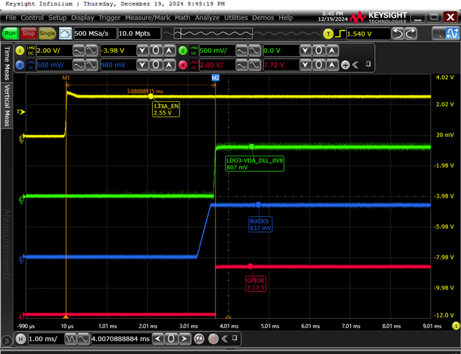
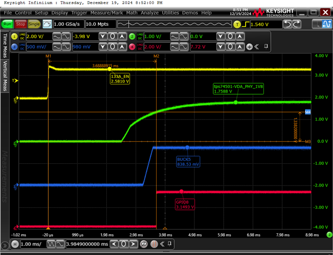
We suspect that we have entered the MCU ONLY mode or PDN-3G or 3M scheme, and also measured the waveform of GPIO8. The waveform of normal and abnormal conditions is as follows.

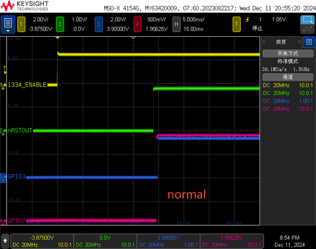
We also suspect that safe to recovery(S2R) mode has been entered, and we also measure SOC_SAFETY_ERRn(GPIO3) and MCU_SAFETY_ERRn(GPIO7), with normal and abnormal waveforms shown.

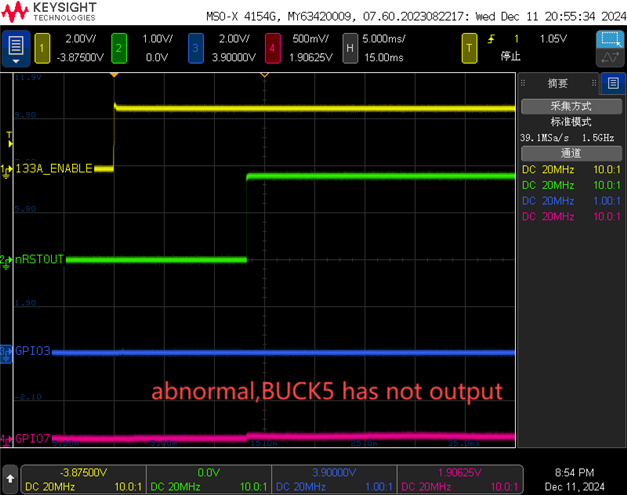
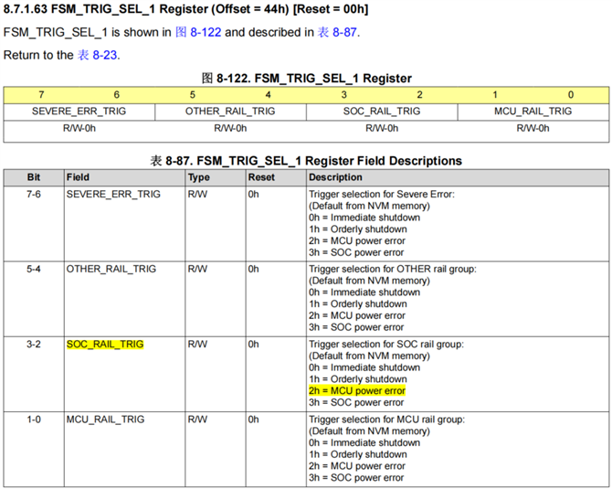
Then we tested manually keeping SOC reset low, When the soc is not working and PMIC's nPWRON/ENABLE=1, the IIC tool was used to write the values of register FSM_TRIG_SEL_1 (address 44H) as 08H, 0AH, 18H and 1AH respectively. these value indicated that bit[3:2]=10, and then kept VCCA powered,After PMIC was enabled again, BUCK5 could not output. The interrupt event did not occur.We provide all read registers for your analysis.

Test condition
Register address VCCA=3.3V and ENABLE=0(NVM value) VCCA=3.3V and ENABLE=1(Normal start but soc is not working) VCCA=3.3V and ENABLE=1(Abnormal start,BUCK5 is not good)
01 82 82 82
02 3A  3A  3A 
03 05 05 05
04 A0  33 33
05 2C  2C  2C 
06 A0  A0  A0 
07 2C  2C  2C 
08 A0  33 33
09 2C  2C  2C 
0A A0  33 33
0B 2B  2B  2B 
0C A0  33 22
0D 1C  1C  1C 
0E 73 73 73
0F 73 73 73
10 73 73 73
11 73 73 73
12 41 41 41
13 41 41 41
14 B2  B2  B2 
15 B2  B2  B2 
16 41 41 41
17 41 41 41
18 1B  1B  1B 
19 1B  1B  1B 
1A 1B  1B  1B 
1B 1B  1B  1B 
1C 1B  1B  1B 
1D A0  31 31
1E A0  31 31
1F A0  31 31
20 A0  31 31
21 00 00 00
22 00 00 00
23 38 38 38
24 74 F4  F4 
25 10 10 10
26 38 38 38
27 1B  1B  1B 
28 3F  3F  3F 
29 1B  1B  1B 
2A 1B  1B  1B 
2B 00 01 01
2C 7F  3F  3F 
2D 00 00 00
2E 00 00 00
2F 00 00 00
30 00 00 00
31 20 20 20
32 40 40 40
33 50 50 50
34 D0  D0  D0 
35 01 01 01
36 03 03 03
37 30 30 30
38 18 18 18
39 48 09 09
3A 10 10 10
3B 43 43 43
3C 01 01 01
3D 00 00 00
3E 00 01 01
3F 00 80 80
40 02 0F  0F 
41 A5  A5  A5 
42 95 95 95
43 01 05 05
44 1A  1E  08
45 01 01 01
46 55 55 55
47 D5  95 95
48 1D  19 19
49 00 00 00
4A 00 00 00
4B 00 00 00
4C 00 00 00
4D 00 00 00
4E 00 00 00
4F FF  FF  FF 
50 FF  FF  FF 
51 3F  3F  3F 
52 11 11 11
53 02 02 02
54 30 30 30
55 00 00 00
56 00 00 00
57 00 00 00
58 00 00 00
59 00 00 00
5A 10 18 9A 
5B 00 00 00
5C 00 00 00
5D 00 00 00
5E 00 00 00
5F 00 00 02
60 00 00 00
61 00 00 04
62 00 00 00
63 00 00 00
64 00 00 00
65 00 02 02
66 01 01 01
67 00 00 00
68 00 00 00
69 00 00 04
6A 00 00 00
6B 00 00 00
6C 00 00 00
6D 00 00 00
6E 00 00 00
6F 00 00 00
70 00 00 00
71 00 00 00
72 00 00 00
73 00 02 02
74 00 00 00
75 00 00 00
76 00 00 00
77 00 00 00
78 00 00 00
79 00 00 00
7A 00 00 00
7B 00 00 00
7C 00 00 00
7D 00 00 00
7E 00 00 00
7F 00 00 00
80 00 00 00
81 00 1B  1B 
82 08 04 04
83 00 00 00
84 0F  0F  0F 
85 00 00 00
86 00 00 00
87 00 00 00
88 00 00 00
89 00 00 00
8A 1F  1F  1F 
8B 0B  0B  0B 
8C FF  FF  FF 
8D FF  FF  FF 
8E 00 00 00
8F 00 00 00
90 00 00 00
91 00 00 00
92 00 00 00
93 00 00 00
94 00 00 00
95 00 00 00
96 00 00 00
97 00 00 00
98 00 00 00
99 00 00 00
9A 00 00 00
9B 00 00 00
9C 00 00 00
9D 00 00 00
9E 00 00 00
9F 00 00 00
A0 00 00 00
A1 00 00 00
A2 00 00 00
A3 80 80 80
A4 00 00 00
A5 00 00 00
A6 08 08 08
A7 00 00 00
A8 00 00 00
A9 00 00 00
AA 00 00 00
AB 00 00 00
AC 00 00 00
AD 00 00 00
AE 00 00 00
AF 00 00 00
B0 00 00 00
B1 00 00 00
B2 00 00 00
B3 00 00 00
B4 00 00 00
B5 00 00 00
B6 00 00 00
B7 00 00 00
B8 01 01 01
B9 01 01 01
BA 00 00 00
BB 00 00 00
BC 00 00 00
BD 00 00 00
BE 00 00 00
BF 00 00 00
C0 00 00 00
C1 00 00 00
C2 00 00 00
C3 60 E0  E0 
C4 80 80 80
C5 00 00 00
C6 00 00 00
C7 00 00 00
C8 00 00 00
C9 00 00 00
CA 00 00 00
CB 00 00 00
CC 00 00 00
CD 2D  2D  2D 
CE 9D  9D  9D 
CF 00 00 00
D0 00 00 00
D1 00 00 00
D2 00 00 00
D3 00 00 00
D4 00 00 00
D5 00 00 00
D6 00 00 00
D7 00 00 00
D8 00 00 00
D9 00 00 00
DA 00 00 00
DB 00 00 00
DC 00 00 00
DD 00 00 00
DE 00 00 00
DF 00 00 00
E0 00 00 00
E1 00 00 00
E2 00 00 00
E3 00 00 00
E4 00 00 00
E5 00 00 00
E6 00 00 00
E7 00 00 00
E8 00 00 00
E9 00 00 00
EA 00 00 00
EB 00 00 00
EC 00 00 00
ED 00 00 00
EE 00 00 00
EF 00 00 00
F0 FB  04 04
F1 4C  06 06
F2 4A  B5  B5 
F3 62 28 28
F4 F6  1F  1F 
F5 33 43 43
F6 29 29 29
F7 4A  4A  4A 
F8 30 30 30
F9 F0  F0  F0 
FA 1F  1F  1F 
FB B1 B1  B1 
FC 00 00 00
FD 00 00 00
FE C1 C1  C1 
FF 76 76 76

If possible, I hope you can verify it by clicking my method on the demo board. The test process is shown in the figure. 

Our hardware circuit completely refers to the J784S4 PDN-3F scheme. I want to know what caused MCU power error. There was no related interruption. However, as long as SOC_RAIL_TRIG is not set to MCU power error, BUCK5 will not be shut down.

We look forward to receiving your reply.

Best Regards,

Xiang Ye

  • Hello,

    sorry,mcu power error occurs occasionally in both normal and abnormal situations, most of which are read as 00H,The read fault is LDO3_SC_INT=1,When the output capacitance of LDO3 was increased by 4.7uf, BUCK5 still had no output.Register values are updated as follows.

    Test condition
    Register address VCCA=3.3V and ENABLE=0(NVM value) VCCA=3.3V and ENABLE=1(Normal start but soc is not working) VCCA=3.3V and ENABLE=1(Abnormal start,BUCK5 is not good) VCCA=3.3V and ENABLE=1(Abnormal start,BUCK5 is not good)
    01 82 82 82 82
    02 3A  3A  3A  3A 
    03 05 05 05 05
    04 A0  33 33 33
    05 2C  2C  2C  2C 
    06 A0  A0  A0  A0 
    07 2C  2C  2C  2C 
    08 A0  33 33 33
    09 2C  2C  2C  2C 
    0A A0  33 33 33
    0B 2B  2B  2B  2B 
    0C A0  33 22 22
    0D 1C  1C  1C  1C 
    0E 73 73 73 73
    0F 73 73 73 73
    10 73 73 73 73
    11 73 73 73 73
    12 41 41 41 41
    13 41 41 41 41
    14 B2  B2  B2  B2 
    15 B2  B2  B2  B2 
    16 41 41 41 41
    17 41 41 41 41
    18 1B  1B  1B  1B 
    19 1B  1B  1B  1B 
    1A 1B  1B  1B  1B 
    1B 1B  1B  1B  1B 
    1C 1B  1B  1B  1B 
    1D A0  31 31 31
    1E A0  31 31 31
    1F A0  31 31 31
    20 A0  31 31 31
    21 00 00 00 00
    22 00 00 00 00
    23 38 38 38 38
    24 74 F4  F4  F4 
    25 10 10 10 10
    26 38 38 38 38
    27 1B  1B  1B  1B 
    28 3F  3F  3F  3F 
    29 1B  1B  1B  1B 
    2A 1B  1B  1B  1B 
    2B 00 01 01 01
    2C 7F  3F  3F  3F 
    2D 00 00 00 00
    2E 00 00 00 00
    2F 00 00 00 00
    30 00 00 00 00
    31 20 20 20 20
    32 40 40 40 40
    33 50 50 50 50
    34 D0  D0  D0  D0 
    35 01 01 01 01
    36 03 03 03 03
    37 30 30 30 30
    38 18 18 18 18
    39 48 09 09 09
    3A 10 10 10 10
    3B 43 43 43 43
    3C 01 01 01 01
    3D 00 00 00 00
    3E 00 01 01 01
    3F 00 80 80 80
    40 02 0F  0F  0F 
    41 A5  A5  A5  A5 
    42 95 95 95 95
    43 01 05 05 05
    44 1A  1E  08 08
    45 01 01 01 01
    46 55 55 55 55
    47 D5  95 95 95
    48 1D  19 19 19
    49 00 00 00 00
    4A 00 00 00 00
    4B 00 00 00 00
    4C 00 00 00 00
    4D 00 00 00 00
    4E 00 00 00 00
    4F FF  FF  FF  FF 
    50 FF  FF  FF  FF 
    51 3F  3F  3F  3F 
    52 11 11 11 11
    53 02 02 02 02
    54 30 30 30 30
    55 00 00 00 00
    56 00 00 00 00
    57 00 00 00 00
    58 00 00 00 00
    59 00 00 00 00
    5A 10 18 18 9A(Both normal and abnormal have occurred)
    5B 00 00 00 00
    5C 00 00 00 00
    5D 00 00 00 00
    5E 00 00 00 00
    5F 00 00 00 02(Both normal and abnormal have occurred)
    60 00 00 00 00
    61 00 00 00 04(Both normal and abnormal have occurred)
    62 00 00 00 00
    63 00 00 00 00
    64 00 00 00 00
    65 00 02 02 02
    66 01 01 01 01
    67 00 00 00 00
    68 00 00 00 00
    69 00 00 00 04(Both normal and abnormal have occurred)
    6A 00 00 00 00
    6B 00 00 00 00
    6C 00 00 00 00
    6D 00 00 00 00
    6E 00 00 00 00
    6F 00 00 00 00
    70 00 00 00 00
    71 00 00 00 00
    72 00 00 00 00
    73 00 02 02 02
    74 00 00 00 00
    75 00 00 00 00
    76 00 00 00 00
    77 00 00 00 00
    78 00 00 00 00
    79 00 00 00 00
    7A 00 00 00 00
    7B 00 00 00 00
    7C 00 00 00 00
    7D 00 00 00 00
    7E 00 00 00 00
    7F 00 00 00 00
    80 00 00 00 00
    81 00 1B  1B  1B 
    82 08 04 04 04
    83 00 00 00 00
    84 0F  0F  0F  0F 
    85 00 00 00 00
    86 00 00 00 00
    87 00 00 00 00
    88 00 00 00 00
    89 00 00 00 00
    8A 1F  1F  1F  1F 
    8B 0B  0B  0B  0B 
    8C FF  FF  FF  FF 
    8D FF  FF  FF  FF 
    8E 00 00 00 00
    8F 00 00 00 00
    90 00 00 00 00
    91 00 00 00 00
    92 00 00 00 00
    93 00 00 00 00
    94 00 00 00 00
    95 00 00 00 00
    96 00 00 00 00
    97 00 00 00 00
    98 00 00 00 00
    99 00 00 00 00
    9A 00 00 00 00
    9B 00 00 00 00
    9C 00 00 00 00
    9D 00 00 00 00
    9E 00 00 00 00
    9F 00 00 00 00
    A0 00 00 00 00
    A1 00 00 00 00
    A2 00 00 00 00
    A3 80 80 80 80
    A4 00 00 00 00
    A5 00 00 00 00
    A6 08 08 08 08
    A7 00 00 00 00
    A8 00 00 00 00
    A9 00 00 00 00
    AA 00 00 00 00
    AB 00 00 00 00
    AC 00 00 00 00
    AD 00 00 00 00
    AE 00 00 00 00
    AF 00 00 00 00
    B0 00 00 00 00
    B1 00 00 00 00
    B2 00 00 00 00
    B3 00 00 00 00
    B4 00 00 00 00
    B5 00 00 00 00
    B6 00 00 00 00
    B7 00 00 00 00
    B8 01 01 01 01
    B9 01 01 01 01
    BA 00 00 00 00
    BB 00 00 00 00
    BC 00 00 00 00
    BD 00 00 00 00
    BE 00 00 00 00
    BF 00 00 00 00
    C0 00 00 00 00
    C1 00 00 00 00
    C2 00 00 00 00
    C3 60 E0  E0  E0 
    C4 80 80 80 80
    C5 00 00 00 00
    C6 00 00 00 00
    C7 00 00 00 00
    C8 00 00 00 00
    C9 00 00 00 00
    CA 00 00 00 00
    CB 00 00 00 00
    CC 00 00 00 00
    CD 2D  2D  2D  2D 
    CE 9D  9D  9D  9D 
    CF 00 00 00 00
    D0 00 00 00 00
    D1 00 00 00 00
    D2 00 00 00 00
    D3 00 00 00 00
    D4 00 00 00 00
    D5 00 00 00 00
    D6 00 00 00 00
    D7 00 00 00 00
    D8 00 00 00 00
    D9 00 00 00 00
    DA 00 00 00 00
    DB 00 00 00 00
    DC 00 00 00 00
    DD 00 00 00 00
    DE 00 00 00 00
    DF 00 00 00 00
    E0 00 00 00 00
    E1 00 00 00 00
    E2 00 00 00 00
    E3 00 00 00 00
    E4 00 00 00 00
    E5 00 00 00 00
    E6 00 00 00 00
    E7 00 00 00 00
    E8 00 00 00 00
    E9 00 00 00 00
    EA 00 00 00 00
    EB 00 00 00 00
    EC 00 00 00 00
    ED 00 00 00 00
    EE 00 00 00 00
    EF 00 00 00 00
    F0 FB  04 04 04
    F1 4C  06 06 06
    F2 4A  B5  B5  B5 
    F3 62 28 28 28
    F4 F6  1F  1F  1F 
    F5 33 43 43 43
    F6 29 29 29 29
    F7 4A  4A  4A  4A 
    F8 30 30 30 30
    F9 F0  F0  F0  F0 
    FA 1F  1F  1F  1F 
    FB B1 B1  B1  B1 
    FC 00 00 00 00
    FD 00 00 00 00
    FE C1 C1  C1  C1 
    FF 76 76 76 76
  • Hi,

    Thanks for reaching out. Let me come to you by tomorrow and need time to look into this. 

    Regards,

    Ishtiaque 

  • Hello Ishtiaque,

    Thanks for your reply. By the way, MCU power error interrupts have occurred both under normal and abnormal conditions of BUCK5, but no matter whether buck5 outputs normally or not, the interrupts did not occur most of the time.

    Best Regards,

    Xiang

  • Hello Ishtiaque,

    Please pay attention to this question when you are free.Thankyou.

    Best Regards,

    Xiang

  • Hello Xiang,

    I work on the same team as Ishtiaque.

    From your initial post, you showed that BUCK5 is not good when GPIO8 goes high ~4ms after Enable and BUCK5 is good when GPIO8 goes high ~8ms after Enable. 

    Why is there a discrepancy between when GPIO8 goes high? 

    The PMIC checks the state of GPIO8 at ~5.7ms after Enable and then sets the SOC_RAIL_TRIG bit field accordingly.

  • Hello Michael,

    Thanks for your reply.

    I'm sorry that the pictures I provided were measured in two different situations. The waveform of BUCK5 when it is good is measured when VCCA power up, and the waveform of BUCK5 when it is not good may include the detection of overvoltage and undervoltage, etc. The waveform of BUCK5 when it is not good is measured when VCCA is always powered, which does not require the detection of overvoltage and undervoltage, indicating that the time is short.

    It doesn't matter anymore,Now I provide the waveform under the constant power supply of VCCA. The only difference now lies in the value of the 44H register. When BUCK5 is good, the value of the register is 1EH, and when it is bad, the value of the register is 08H.

    In terms of timing, there is no difference. GPIO8 can be started normally even when it is set to high level before ~5.7ms.

    Please let me know if there are any other waveforms or schematics you would like to see.

    I'm looking forward to your next reply, thank you.

    Best Regards,

    Xiang

  • It doesn't matter anymore,Now I provide the waveform under the constant power supply of VCCA. The only difference now lies in the value of the 44H register. When BUCK5 is good, the value of the register is 1EH, and when it is bad, the value of the register is 08H.

    Is your software writing to register 0x44 at any point? During first power up, when Enable is set HIGH for the first time, the PMIC's PFSM will set the value of SOC_RAIL_TRIG based on GPIO8 status at the 5.7ms mark. BUCK5 is then included in the To_ACTIVE sequence based on whether SOC_RAIL_TRIG = 2h or 3h. 

    Can you replace channel 2 (green) with VCCA and show the behavior of the first power up attempt?

  • Hello Michael,

    Thanks for your reply.

    First on the first power-on, the enable is set to high and everything is fine because register 44H is the NVM value (1EH) at this time. At this time, VCCA always keeps the power supply, and we only modify the value of this register to (08H) and then set the enable to low and then high. buck5 is not good.

    Since VCCA is always provided as 3.3V after being powered on, the waveform is always a straight line. If you need it, I can provide it tomorrow.

    BR,

    Xiang

  • First on the first power-on, the enable is set to high and everything is fine because register 44H is the NVM value (1EH) at this time. At this time, VCCA always keeps the power supply, and we only modify the value of this register to (08H) and then set the enable to low and then high. buck5 is not good.

    Why are you modifying this register? The PFSM reads this register and includes BUCK5 in the power up sequence based on the value of the SOC_RAIL_TRIG bitfield.

    If you do not want the PMIC to react to an SOC_PWR_ERR event, then use registers 0x41, 0x42, and 0x43 to set all the rails to the MCU rail group after boot.

  • Hello Michael,

    Thanks for your reply.

    I am in charge of hardware, and this register was modified by a software colleague to solve a certain problem. We have always believed that there was an MCU power error. I roughly understand what you mean. If MCU power error occurs, gpio8 will be set to high in advance. After the VCCA is powered on for the first time, the gpio8 status setting SOC_RAIL_TRIG = 2h or 3h is read 5.7ms after the enable setting is set to high. Because our software has written the register value as 2h, in the case that VCCA always keeps 3.3V unchanged, that is, the register value will not be lost after writing, and the state of gpio8 will not be read after enable is set to a high value. Since SOC_RAIL_TRIG = 2h, pmic believes that MCU power error event has occurred and will shut down BUCK5, which has the same effect as when the enable is set to high for the first power-on and then 5.7ms to read gpio8=1. Is my understanding correct?

    BR,

    Xiang

  • I would re-word this sentence to make it correct.

    Since SOC_RAIL_TRIG = 2h, pmic believes that MCU power error event has occurred and will shut down BUCK5, which has the same effect as when the enable is set to high for the first power-on and then 5.7ms to read gpio8=1.

     Since SOC_RAIL_TRIG = 2h, pmic believes that it is operating in the combined power group scenario (PDN-3G to PDN-3M) and will not include BUCK5 in it's power up sequence , which has the same effect as when the enable is set to high for the first power-on and then 5.7ms to read gpio8=1.