This thread has been locked.
If you have a related question, please click the "Ask a related question" button in the top right corner. The newly created question will be automatically linked to this question.
Tool/software:
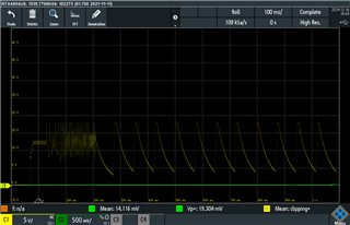
I've been handed a design from a coworker who no longer works at our company and I'm very new to power electronics. We tweaked the previous design (which is functional and can be used for reference) to adjust the input and output voltages but kept the major architecture the same. Input voltage range is now from 30-45V with an output voltage of 12 VDC. I think we are pretty close but something seems off just enough to make things unstable. The image below shows the output waveform trying to give us 12V before going haywire. What would you pros recommend I try to isolate and fix the issue? Any other specific information that would be helpful?
Hello,
If you could tell me the following it will help troubleshoot your issues.
1. What is the input and output power requirments of the original design?
2. What is the input and power requirements of the original design?
3. What did you change in the new dedsign to make it work at this new power range?
Regards,
The original design was using 54-70V input voltage range and 28V output. Both designs are targeting 250W output capability although my power requirements are not strict. I'll simply inform maximum power output with whatever we can achieve for now.
To change the input and output voltage range we adjusted the compensation feedback signal voltage divider, the microcontroller voltage and current feedback loops (for load sharing control with multiple devices in parallel), and the microcontroller software to match. The microcontroller really only provides the UVLO signal as a sort of enable signal and trims the comp signal for tuning of the load sharing.
We also copied the design from one design environment to another using new library components and we have already found and corrected several mistakes from that process. There is a good chance there may still be more mistakes (both in the schematic and in the layoute/route).
Update: Today I removed the Comp feedback signal to give it maximum duty cycle and got a stable 19.36 VDC output. It's looking like something isn't quite right with my feedback loop. I'll be digging into that deeper.
Hello,
Thanks for the information and letting me know.
If you need any more questions or help let us know?
Regards,