Tool/software:
Dear
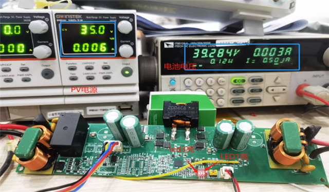
At present, there are problems with the MPPT module debugging. Attached are the schematic diagram and PCB
The main issues are as follows:
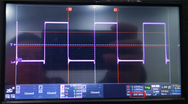
When MOS is not soldered, the gate waveform of (Q5, Q6) is normal, as shown in the following figure:
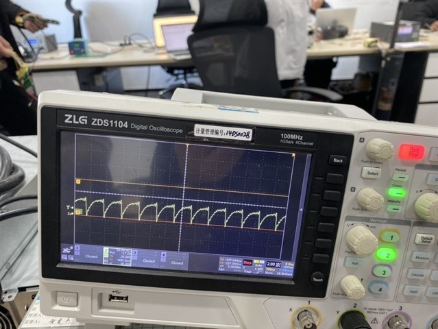
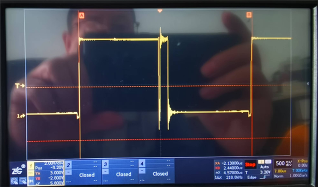
After welding Q5 (single MOS), the waveform distortion is severe, as shown in the following figure
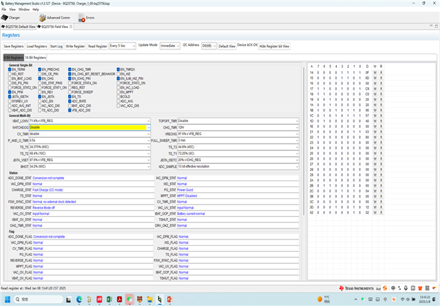
Through I2C and BQ studio tools, we have checked the chip's working status and found that it is normal. Please help us investigate the issue as soon as possible.
Additionally, could you please help us evaluate a few issues
Q1. What is the maximum distance that BQ25756's driver can support? (Distance between IC and MOSFET)
Q2. Does the BQ25756 chip solution not support double-sided PCB? Do I have to use multi-layer boards?
Q3. Is it best to use surface mount MOSFETs? Can't it be packaged with TO-220? thanks.