This thread has been locked.

If you have a related question, please click the "Ask a related question" button in the top right corner. The newly created question will be automatically linked to this question.

TPS40210: Boost - very high losses in MOSFET at load

Part Number: TPS40210

Tool/software:

i tryed to creat quick&dirty boost for nixie tubes with TPS40210, use TPS4021x_Boost_Quickstart_Calculator.xlsx for all paramters

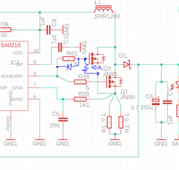
This is the shematic:
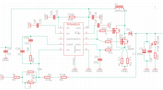
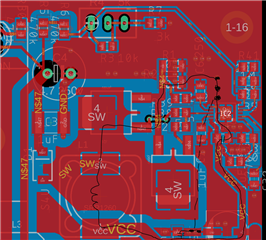


and this is PCB:


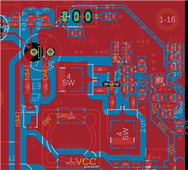
the boos work very well without load, from 12v get only 15ma, output voltage is stable and clean between 100 and 200v with or without load.

but with small load losess rise rapudly, at 2w load it take 3.6W, at 4.5w load - 11W !! i use two mosfets with 500v 0.6A (AOD9N40)
Inductor is 100uH with 8.5a saturage and 4.5A heat current. Inductor is every time cool.
Filter capacitor - 1uF/500v ceramic + 10uF elco

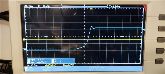
yellow at current sense resistor with 0.05 ohm, get with springs on


Blue - on MOSFET source with 110v output and 20mA load

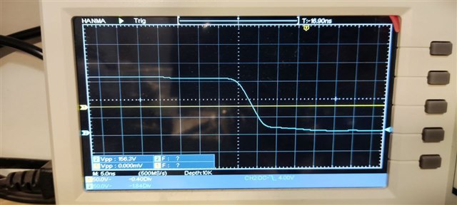
with more magnification:


Output voltage is still stable, but losses at MOSFET are very high, what it the problem ?

  • Hello I R,

    Thanks for using the e2e forum and sharing schematic and layout.
    There are some comments on they layout which may be related for the bad performance:

    - You are using thermal relieve pads. This makes soldering easier, but has a very bad influence on the system performance, especially for the power stage, as it creates bottlenecks for the main current paths. It is recommended to avoid thermal relieve pads.
    - The shunt resistor could be placed a bit closer to the MOSFETs
    - The return path of the input loop via ground seems rather long and might even run directly below the IC. (VIN caps -> inductor -> MOSFET -> shunt -> VIN cap)
    The output loop looks okay

    You can also consider adding more output capacitance to reduce the switching noise coupled into the output voltage.

    Please let me know if you have additional questions.
    Best regards,
    Niklas

  • The output voltage is very clean and stable up to 55mA at 150v (i can not test more right now, MOSFETs are going very hot)

    current sense resistor is ~2mm away from one mosfet and 12mm from the second, but my first test was with only first mosfet
    and i see no switching noise on inductor, only strange noises on current sensing

    Can you paint wich return path yop mean

    My proble is that output voltage is very stable, but MOSFET losses are very high and i don't know why,

    this is my inductor with 4.5A saturation current : https://www.lcsc.com/product-detail/Power-Inductors_SHOU-HAN-CYA1265-100UH_C19268674.html

    MOSFETs 400v 0.8 ohm:
    https://www.aosmd.com/products/mosfets/medium-voltage-mosfets-40v-400v/aod9n40
    Diode is US1M https://www.vishay.com/docs/88768/us1_test_dcicons.pdf

    are MOSFET and diode not fast enought ?

  • ok, i try with lowe frequence, now it is 108-109KHz

    Load is 46ma at 150v, 6,9W, consumption 12v 0.75A, 9W, Efficiency 76%

  • with 20V input at 108KHz - Effecincy 81% ...

  • Hi I R,

    Thanks for the feedback.
    With the thermal relieve pad and the 2mm traces at the sense resistor, you add inductive parasitics into the system.
    I am not fully sure yet if this is the root cause for the strong MOSFET heat-up, but it is definitely not ideal for the system.

    I marked the input loop on the schematic with a black line. (dotted line means the GND path on the other layers)

    Can you give me your Vin range, Vout and maximum load current parameters?
    With this data it is easier to check if inductor/MOSFET/diode are suitable.

    Best regards,
    Niklas

  • Vin now is12v, but may be i will use power supply from notebook with 19.5v.

    Load should be 150v / 50-100ma, typically 80mA

    Now i have no idea how i can route correct this on 2 side PCB ... example from the datasheet is for 4 layer PCB :(
    i will try.
    But as you wrote - i think too that it is more important for stability, not for heating losses ..

    Two MOSFETs are only for thes case, if RdsOn of one is too high, it exist not so much not expensive MOSFETs with 300-400v and low RdsOn in smd cases.

  • Hi I R,

    Thanks for the quick reply.
    There is another major issue I see with these input - output specs.
    From 12V to 150V, you have a very high boost factor.
    At no load operation, this is still possible as you run in DCM and the duty cycle is smaller.
    When increasing the load, duty cycle increases up to ~ 92% when it enters CCM operation.
    This might also be related to why the system fails with increased load.
    We generally recommend a maximum boost factor of 7x or 8x times the input voltage.

    A safer solution would be a flyback topology, which can achieve higher boost ratios due the different winding ratios.

    Best regards,
    Niklas

  • It exist a lot of projects Boot from 12 to 180-220v for diverse nixie projects, like this big one :

    https://neonkev.com/2019/10/15/success-201-boost-at-40-watts-without-a-transformer/

    but i want to buld my small quick i dirty :) and my still not work from 19.5v too
    I don't know what is the problem for poor eeficency, may be i need SiC Schottky diode for 300KHz and 200v output
    It look like that rise is too clow, over 50-75nc ... like ultrafst diode Trr :(

  • now is inductor 200uH, 110JHz, it work at 12.5W output power but still poor efficiency, consume nearly 18W, also only 70%
    with two MOSFET in parallel each 0.8 ohm Disappointed

  • Hi I R,

    Thanks for referencing to other projects. I was not aware of this.

    If the main power loss still come from the MOSFET, changing the schottky diode might not solve the low efficiency.
    Can you make a waveform measurement of the switch node signal?
    So you have have only share the driver and current sense signal.

    Thanks and best regards,
    Niklas

  • now i have only one MOSFET 9N40, and at drain-inductor-diode point i can get 20nc rise and 5nc fall time

    but efficiency is still poor, it mosfet is cold i have 82-84% but if it will be hotter - efficiency go down to 74-70%


    But i have redesign all ground connection as you describe as short as possible, replace MOSFET to STD33N60M2 with 600v / 0.125 Ohm, and ordered new PCB ..

    Will see how it will work ...

  • Hi I R,

    Looking at the waveforms, there is one additional notice I have not commented on so far.
    The rise time of the SW takes about ~40ns. This is when the MOSFET gate is closing. The fall time only takes ~5ns.
    The long rise time may add to the losses, so common designs speed up the rise time of SW either by adding a 10kOhm resistor from gate to source, or by adding a diode in parallel to the gate resistor.


    This can lead to worse EMI performance, but could increase efficiency.

    Best regards,
    Niklas

  • Thank you for you help
    I reworked the board

    now is ground from both side as short as possible, i hope ...


    I change the MOSFET to stb33n60m2 https://www.mouser.de/datasheet/2/389/stb33n60m2-1850311.pdf
    600v and only 0.1 Ohm, but heavier gate

    Reduce frequnce to 100KHz ...
    Inductor is 2x100uH 4.5A

    and now it i less stable i same efficiency 75-80% only...

    and ofter it won't start anymore, just generate burs of impulses and restart


    i have no idea any more, everething was checked with, better than data from TPS4021x_Boost_Quickstart_Calculator.xlsx

  • Hi I R,

    I am sorry to hear the efficiency and stability issues did not improve.
    The burst switching could also be the regular light load behavior. If the minimum on-time gets too low, the device will switch in bursts and the stops for a longer period of time. But this should only occur if the output target voltage is already reached.

    The device has a minimum switching frequency of 35kHz according to datasheet.
    Have you considered going even lower than 100kHz to reduce switching losses?

    Best regards,
    Niklas