This thread has been locked.

If you have a related question, please click the "Ask a related question" button in the top right corner. The newly created question will be automatically linked to this question.

LMZM23601: Minimum value of maximum duty cycle

Part Number: LMZM23601
Other Parts Discussed in Thread: TPSM33625

Tool/software:

Dear Sirs and Madams,

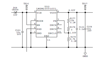
We are currently verifying the operation of LMZM23601.
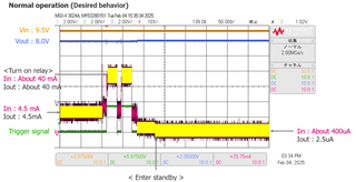
VOUT:8V

IOUT:2.5uA

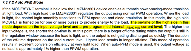
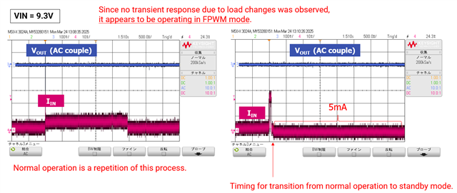
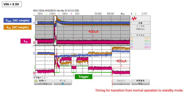
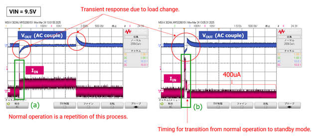
Currently, for all products, when VIN is 9.6V, the input current is approximately 400uA.

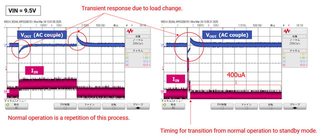
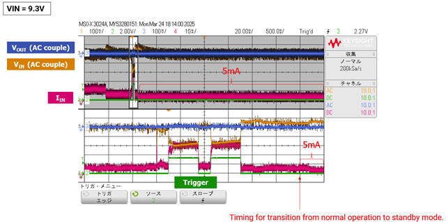
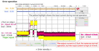
However, we found that when VIN was 9.5V, there were some products with an input current of approximately 400uA and other products with an input current of 4.5mA to 5mA.

When I checked the maximum duty cycle on the data sheet, it was 91% (typ), but what is the expected minimum value?

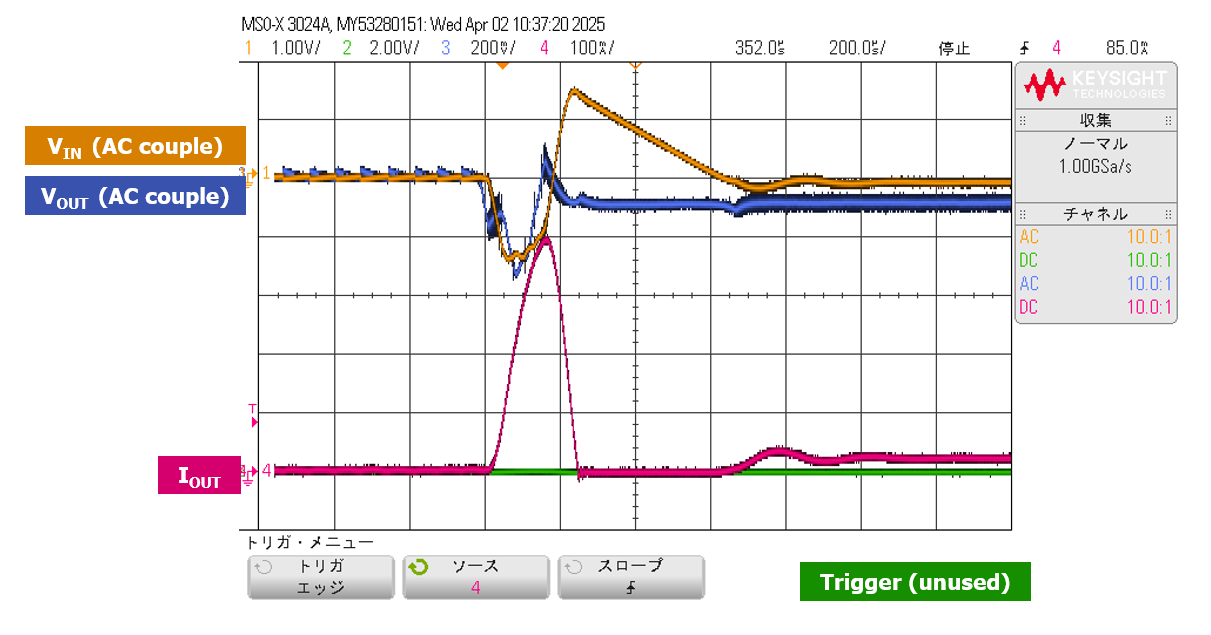
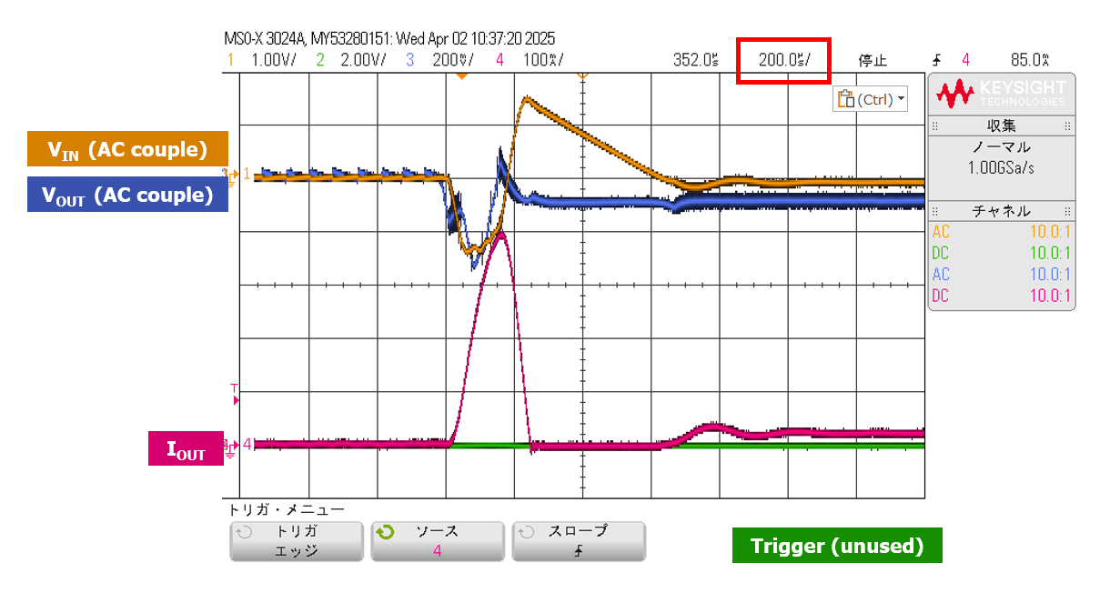
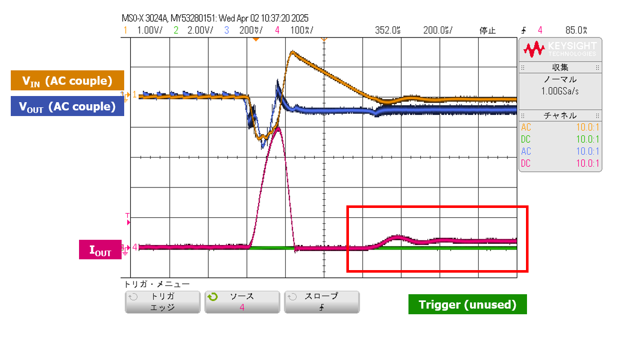
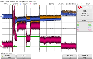
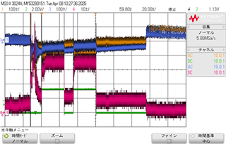
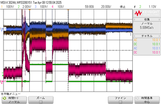
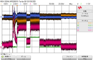
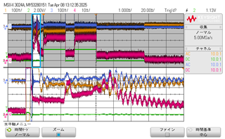
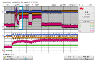
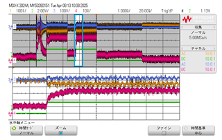
When observing the output voltage, we can see that there is a difference in the switching period.

[ VIN = 9.5V to 9.6V, IIN = 400uA ]

The switching frequency is about 1kHz (1ms).

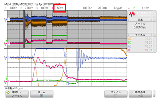
[ VIN = 9.5V, IIN = 4.5mA to 5mA ]

The switching frequency is about 66kHz? (15us?).

The load current is 2.5uA for both of the waveforms above.

In the waveform below, I suspect that the cause of the increase in input current (IIN) is that the high-side FET is not completely saturated right?

Please could you provide us your opinion on the cause of this issue.

Regards,

Masashi

  • Hi Masashi, 

    Could you please help me with the following information for better understanding?

     You are operating nearly at 84.25% duty. May I know for what reason you need the min duty information?

     How are you measuring the input current? I assume this is the average input current. For Vout=8V, Iout=2.5uA, and Vin=9.5V; Iin=4-5mA seems pretty high. Could you please share the waveforms of Iin and Iout as well with Vout for better understanding the issue?

    Regards

    Arpita

  • Hello Arpita,

    I thought the problem was that the input current was increasing as the input voltage decreased, so I wanted to know the minimum value of Dmax.

    We will obtain the waveforms of Vout, Iin, and Iout and report them later.

    Regards,

    Masashi

  • Hello Masashi,

    Could you please probe the waveforms during this transition also: Vin 9.6V to 9.5V, Iin 400uA to 4-5mA in oscilloscope and share with us?

  • Hello Arpita,

    We ask our customer to obtain the waveforms (Vout(9.5V/9.6V/9.6V to 9.5V), Iin and Iout ).

    After I get these waveforms I will report back to this thread.

    Regards,

    Masashi

  • Hello Arpita,

    We are currently requesting waveform acquisition, but do you know what value is set for IPEAK-MIN current level in the highlighted sentence below in the data sheet?

    Regards,

    Masashi

  • Hi Masashi,

    I will check this data internally and get back to you within couple of days. 

    Regards

    Arpita

  • Hello Arpita,

    Do you have any update?

    Now, I am confirming the measurement data I received from the customer.

    I will contact you as soon as I have it compiled.

    Regards,

    Masashi

  • Hi Masashi,

    I have ordered the EVM and I will get back to you once the I get the results/data.

    Do you have any update regarding the waveforms during the transition?

    Regards

    Arpita

  • Hello Arpita,

    I have attached a PowerPoint file summarizing the waveforms for the problematic operation of the LMZM23601.

    The customer is using a digital multimeter for the load current because the current is too small to be measured with an oscilloscope.

    LMZM23601_waveform.pptx

    The LMZM23601 that the customer measured this time works normally up to an input voltage of 9.5V, but when the input voltage drops to 9.3V, the input current does not drop.

    There seem to be a variety of cases, including some that occur when the input voltage drops from 9.6V to 9.5V, and others that occur when the input voltage drops from 9.5V to 9.3V.

    The results of this measurement are the latter.

    Because the LMZM23601 is being used in a battery application, the customer wants it to operate with low current draw without abnormal conditions from input voltages ranging from 9.3V to 16.8V.

    If you have any questions or need any information please feel free to contact us.

    Regards,

    Masashi

  • Hi Masashi,

    I have tested and confirmed in the EVM. Please note that this behavior is expected in low drop-out mode. As Vin reduces nearly to Vout> initially Vout starts falling as the internal Error Amplifier initially tries to maintain previous duty >COMP increases> COMP min threshold is crossed, thus the mode shifts to FPWM, even at very light load. While operating on FPWM mode at low load, the efficiency decreases (Refer to datasheet).  Do you have any further concerns regarding this?

    Regards

    Arpita

  • Hello Arpita,

    Customers want an operation in which the input current does not increase even when the input voltage decreases.

    Is there a way to avoid this issue?

    Regards,

    Masashi

  • Hi Masashi,

    May I know for how long your input is expected to be around ~9.3V-9.5V (where it shifts mode)? If it is for very less time (few ms), then overall efficiency should not be a concern. What is the nominal input voltage?

    Meanwhile, I am checking other variants/buck controller also. I will get back to you in one or two days.

    Regards

    Arpita

  • Masashi,

    Also please let me know what is your full-load output current? 

    Regards

    Arpita

  • Hello Arpita,

    Normal input voltage is 12V, 9.5V to 16.8V.

    full-load output current is about 30mA to 40mA. typically 10mA.

    The customer said that there are individual differences in the input voltage that triggers this FPWM operation, and the customer was concerned that it could occur even at high voltages such as 10V.

    So We would like to know the minimum value for the maximum duty cycle of this module.

    Regards,

    Masashi

  • Hi Masashi,

    May I know for how long your input is expected to be around ~9.3V-9.5V (where it shifts mode)?

    If Vin is expected to stay ~9.5V for very less time (few ms), the overall efficiency should not be a concern as your nominal Vin=12V. For current mode devices, it is difficult to maintain PFM in drop-out region for the operating conditions, as I have explained above.

    Could you please let me know what is the concern with the mode-shifting behavior?

    The device enters into FPWM mode in low drop-out region [vin=~9.3V to 9.5V.] The difference in Vin that you see is ~200mV, which could happen due to part to part variations. The device should not enter into FPWM at Vin=10V at light load.

    From datasheet, it seems like we don't provide this kind of data for this device. However, I will try to check internally if min. value of maximum duty cycle of this can be provided.

    Regards

    Arpita

  • Hello Arpita,

    May I know for how long your input is expected to be around ~9.3V-9.5V (where it shifts mode)?

    The time is short because it is the lower limit voltage of the battery.

    Could you please let me know what is the concern with the mode-shifting behavior?

    Customers are concerned about the timing of this mode at what input voltage.

    Therefore, We would like to know what the minimum maximum duty cycle is expected for the device.

    Also, we have heard that the TPSM33625 does not enter this mode.

    Regards,

    Masashi

  • Hi Masashi

    Could you please provide specific time duration for further discussion?

    As long as the dropout performance of TPSM33625 is acceptable for your application, this looks good and expected from our end. 

    Regards

    Arpita

  • Hello Arpita,

    I apologize for taking so long.

    If it is difficult to identify the threshold at which FPWM operation occurs when the input voltage drops, the customer would like to know if when the LMZM23601 has an input voltage of 10V and an output voltage of 8V, it will remain in PFM operation and will not operate in this type of FPWM mode.

    Regards,

    Masashi

  • Hi Masashi,

    I will check on the EVM and let you know the result in couple of days.

    Thank you

  • Hello Arpita,

    I would like to confirm something from your past questions.

    Yor said "May I know for how long your input is expected to be around ~9.3V-9.5V (where it shifts mode)? If it is for very less time (few ms), then overall efficiency should not be a concern. What is the nominal input voltage?"

    What I meant in my answer was that as the battery voltage gradually decreases, from 10V to 9.5V to 9.3V, PFM operation cannot be maintained and the controller switches to FPWM, which increases power consumption and shortens the operating time.

    Is the intent of your question consistent with my answer?

    By any chance you were asking in terms of momentary low voltage of the battery and time to recovery after low voltage?

    We only need to know the input voltage at which PFM operation will not change to PWM operation when the output voltage is set to 8V and the load is extremely light, but we would like to know if this problem can be avoided if the input voltage is 10V.

    Regards,

    Masashi

  • Hello Masashi, 

    I have checked in EVM. I do not observe the mode shifting at Vin=10V, Vout=8V, at very light load in EVM. However, I will confirm with design team for the margins. I will get back to you once I hear from them.

    I would like to know "in terms of momentary low voltage of the battery and time to recovery after low voltage"? If the time to recovery after low input voltage is very less/momentary, I don't think the increased power consumption will affect the overall system efficiency. 

    Thanks

    Arpita

  • Hello Arpita,

    Do you have any update?

    Below are the waveforms that were investigated to determine the drop in input voltage in response to your answer.

    You can see the difference in operation when Vin=9.5V and when Vin=9.3V.

    Since it is difficult to read the current value from an oscilloscope, the values ​​shown are those obtained using a digital multimeter.

    Regards,

    Masashi

  • Hi Masashi,

    Apologies for the delay. I am yet to get the data. It might take one-two more days.  As I have said previously it is very difficult to calculate and dependent on other conditions.

    However, I asked   "in terms of momentary low voltage of the battery and time to recovery after low voltage" It would be helpful for me in understanding the concern about efficiency if you can let me know this clearly.

    Regards

    Arpita

  • Hello Arpita,

    The waveform obtained by adding the input voltage (battery voltage) to the waveform in the previous thread is shown below.

    The input voltage and output voltage are set to AC so that voltage fluctuations are easy to understand.

    And one division of the input and output voltage is 100mV.

    Please contact us if you have any information you would like.

    Regards,

    Masashi

  • Masashi,

    Thanks for the complete waveform. Can you please share your schematic for double-check? May I know what are the input capacitors you have used? What is the slew rate of load transient?

    Regards

    Arpita

  • Hi Arpita,

    Our customers provided us with information.

    1.

    Can you please share your schematic for double-check? May I know what are the input capacitors you have used?

    [Ans]

    Input capasitor is 10uF/50V ceramic capasitor.

    2.

    What is the slew rate of load transient?

    [Ans]

    Channel 4 (Red) is an enlarged waveform of the input current.

    The time axis is 1ms/div, and the current value is 10mA/div.

    Input current slew rate is about 35mA - 15mA / 0.5ms = 40mA / ms.

    I request the customer to confirm the output current transient.

    Regards,

    Masashi

  • Hi Masashi,

    Thanks for the information. The schematic looks good. As I have told previously, it is very difficult to calculate the entry point (where mode shifts) of vin exactly, and the behavior of mode changing is quite expected behavior, let me check internally if I can get the data (if any).

    Regards

    Arpita

  • Hello Arpita,

    The load change transient response waveform is attached below.

    Channel 4 (Red) is an enlarged waveform of the output current.

    The time axis is 200us/div, and the current value is 100mA/div.

    Input current slew rate is about 400mA / 160us = 2.5mA / us.

    Regards,

    Masashi

  • Masashi,

    Your previous waveforms and the latest waveforms looks like they have taken in different instants/test conditions.

     Please get back to us once you have vin,vout, iout, Iin captured in single waveform , as I have asked in my previous replies. It will be helpful to debug further and rule out any other issue.

    Regards

    Arpita

  • Hello Arpita,

    Until now, I had only been observing the current on the input side, but when I maximized the waveform of the load fluctuation on the output side (Iout), I found that it was the waveform I have attached.

    Because it is a fast, instantaneous fluctuation, it may not be possible to observe it on the input side.

    Regards,

    Masashi

  • Masashi, 

    Please try to capture Vin, Vout, I out, Iin in single waveform as I have asked before for better understanding.

    However, I have already requested for the data internally, I will get back to you once I hear from them.

    Regards

    Arpita

  • Hello Arpita,

    When you say slew rate, what timing load change slew rate do you mean?

    (a) Load change during normal operation

    (b) Timing for driving the relay before transitioning to standby mode

    The waveform we are sending is a load fluctuation waveform under normal operation (a).

    The customer's normal operation is approximately 0 to 50mA load variation.

    In other words, the red frame in the sent waveform corresponds.

    The slew rate is 50mA/200us = 250uA/us.

    Does this mean that the output current fluctuation waveform under condition (b) is absolutely necessary?

    Similarly, regarding the single waveform you mention, which timing waveform do you need?

    Regards,

    Masashi

  • Masashi,

    As the concerned is regarding the instant (b), It is better if you can share waveforms of Vin,In,Iout,Vout captured during the instant (b) in single waveform at 1) Vin=9.5V 2) Vin=9.3V. Iout waveform during instant (b) is necessary to check what is the exact Iout during the instant (b) when Vin is 9.5V and Vin =9.3V

  • Hello Arpita,

    Please let us confirm your request.

    Since you wish to obtain individual waveforms, does that mean you need a waveform like (B) instead of (A) as before?

    Regards,

    Masashi

  • Masashi,

    Please try to capture like below and share if you can get the waveform like this. However, I will get back to you once I hear from design team internally. 

  • Hello Arpita,

    If there were two current probes, it might be possible to fit the waveform on one sheet, but since there is probably only one current probe, it may be two sheets, Iin and Iout.

    I will ask the customer to retrieve these waveform.

    Regards

    Masashi

  • Hello Arpita,

    Because there is only one current probe, there will be two waveform images, Iin and Iout.

    (A-1) Vin = 9.5V (Yellow), Vout (Blue), Iin (Red)

    (A-2) Vin = 9.5V,(Yellow), Vout (Blue), Iout (Red)

    (B-1) Vin = 9.3V (Yellow), Vout (Blue), Iin (Red)

    (B-2) Vin = 9.3V (Yellow), Vout (Blue), Iout (Red)

    We feel that there are no major differences in the above waveforms.

    The waveform shown below is an enlarged version of the light blue part of the B-2 waveform.

    (B-2-1) Vin = 9.3V (Yellow), Vout (Blue), Iout (Red)

    (B-2-1-1) A waveform that is further expanded from B-2-1, The current division is 50mA/div, which is very different from the others.

    (B-2-2) Vin = 9.3V (Yellow), Vout (Blue), Iout (Red)

    (B-2-3) Vin = 9.3V (Yellow), Vout (Blue), Iout (Red)

    Please understand that due to the resolution of the current probe, it may be difficult to observe currents on the order of microamperes.

    When the input voltage is 9.3V, the waveform appears to show an improved transient response, but please note that this is FPWM rather than PFM.

    When the input voltage is 10V and the output voltage is 8V, are there any indicators that the current will not switch to FPWM operation if the fluctuation from XXmA to YYm A is less than ZZ mA/us?

    Regards,

    Masashi

  • Hi Masashi,

    Apologies for delayed response as I was OOO. I will check and get back to you by tomorrow IST.

  • Hi Masashi,

    Could you please clarify what is XXma/YYma/ZZma?

    It is difficult to understand from the waveforms as the resolution is very low.

    However, as I have already explained in detailed that the behavior what you see is quite expected during drop-out, it seems like we can't do much about the dropout mode of operation.

    I don't feel there is any issue even if the device shifts mode near dropout as this is quite expected and cannot be avoided.

    Regarding the exact Vin when device shifts mode is very difficult to calculate, as I said previously. Still, I am checking internally, will get back to you if I can get any data.

     Otherwise, as I have already suggested, you may want to explore other devices like https://www.ti.com/product/TPSM33625 if their dropout performance is acceptable for you. 

    Regards

    Arpita

  • Hello Arpita,

    Our customer has already completed the design and is therefore unable to change the module.

    So We just want to know what input voltage the LTZM23601 can maintain PFM at when its output voltage is 8V.

    As far as we can tell from checking with a digital multimeter, when the standby (idle load) is around 2.5uA, the input current is around 400uA when the input voltage is 9.5V, but we know that the input voltage is around 4.5mA when the input voltage is 9.3V.

    Is it possible to tell us whether PFM can be maintained under these conditions when the input is 10V, regardless of load fluctuations?

    Regards,

    Masashi

  • Hi Masashi,

     I have checked in one unit of LMZM23601 EVM, and it is not shifting mode at Vin=10V and Vout=8V. 

    As I have already said, it is very difficult to say directly at what Vin the mode shift will occur over the range of operating conditions. I have checked. It looks like we don't provide this kind of data directly. 

    Regards

    Arpita

  • Hello Arpita,

    I would like to thank you for your long-term support regarding this issue.

    We will close this case for now.

    Regards,

    Masashi

  • Hi Masashi,

    Is it possible to tell us whether PFM can be maintained under these conditions when the input is 10V, regardless of load fluctuations?

    Kindly note that, as I have said, it is very difficult to say directly. It requires thorough testing and validation from customer side.

    However, I would like to highlight that the device should work fine even if mode shifts and there should not be any issue from the converter side even if it shifts mode when Vin is near to vout.

    Closing the thread.

    Regards

    Arpita