This thread has been locked.

If you have a related question, please click the "Ask a related question" button in the top right corner. The newly created question will be automatically linked to this question.

TPS54160: Oscillations During Shutdown Causing Downstream Component Failures

Part Number: TPS54160

Tool/software:

Hello,

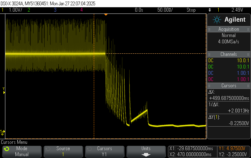
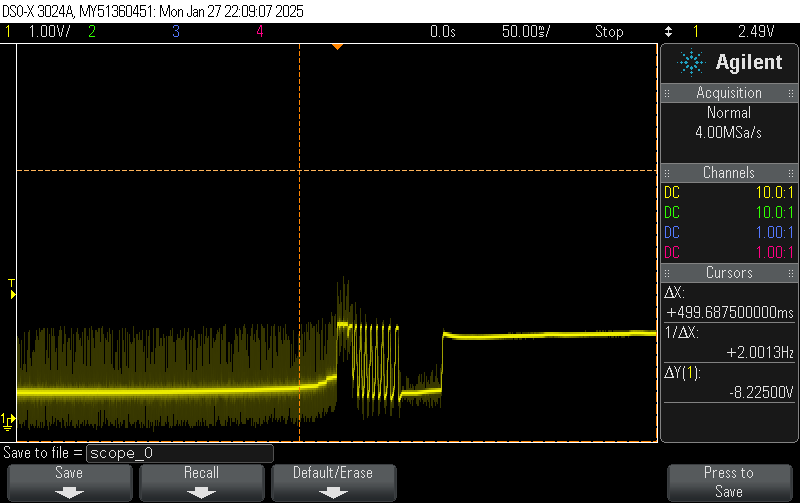
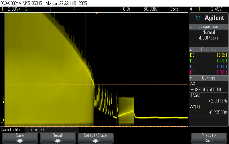
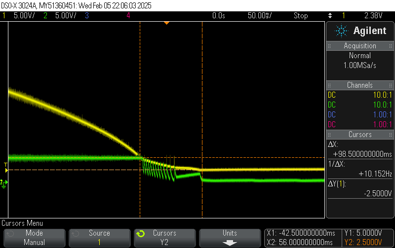
I am experiencing oscillations in my circuit using the TPS54160ADRCR DC/DC converter. The oscillations have a frequency of approximately 200 Hz and last for about 20 cycles. These oscillations occur specifically during shutdown when the input 24VDC drops.

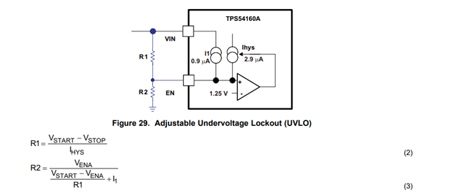
After simulating my design with TI Webench, I discovered that several component values in my current setup are out of the recommended range. Specifically:

  • Output Capacitors: I currently have a 1µF capacitor in parallel with a 22µF capacitor. The datasheet recommends a minimum of 25.3µF to maintain output voltage regulation during unload transients. Webench suggests using two 47µF capacitors.
  • Inductor: The current value is 3.3µH.
  • Input Capacitor: The current value is 1µF.

These oscillations are affecting downstream components, such as the regulators to 3.3V, and may be causing damage to the final op-amp and other components.

I am attaching the schematics of this relevant part of the design for reference. Could the incorrect values of these components be the source of the oscillations I am observing during shutdown? 

Thank you for your assistance.

  • Hi Alex

    Thanks for writing to us!

    The get more information about your design could you please fill the QuickStart for the device?

    Additionally, following waveform will aid in debugging the issue. Could you please capture them?

    1. SW node
    2. Vout
    3. COMP

    Thank you

    Regards

    Onkar

  • Here is link of QuickStart for your reference - SLVC432 Calculation tool | TI.com

  • Hello Onkar

    Copy of TPS54x40_AND_TPS54x60_CALCTOOL_v1p1.xls

    Currently filled (I hope correctly) SLVC432 calculation tool.

    Thank you

    Alex

  • HI Alex

    I review it and get back to you on this by EOD

    Thank you

    Regards

    Onkar Bhakare

  • Hi Alex 

    I reviewed your schematic. Here are my comments

    1. Loop is unstable with selected values of components. Try replacing C7 in your schematic with 470 pF.
    2. Inductor value is small. You can keep inductor value close to the value suggested by the calculator

    Rest looks fine to me. Let me know if this works.

    Here is the QuickStart for your reference - TPS54x40_AND_TPS54x60_CALCTOOL_v2.xlsx

    Disclaimer - This is beta version; I have added frequency response plot in existing calculator

    I hope this helps

    Thank you

    Regards

    Onkar Bhakare

  • Hello Onkar

    Thank you for your guidance regarding the debug process. As requested, I have captured the waveforms for the following nodes:

    1. Vout (first)
    2. COMP (second)
    3. PH (third)


    Thank you

    Alex

  • Hello Alex

    Thanks for sharing the waveform

    Whether this result obtained after changing components to suggested values?

    A simple solution to solve this would be to implementing Vin UVLO. You can add resistive ladder at EN as shown in picture below. Keep Vstart and Vstop voltage levels well below the minimum operating Vin in your application

    For more details, you can refer datasheet section - 8.3.9 Enable and Adjusting Undervoltage Lockout 

    Let me know if need any clarification or further help on this.

    Thank you

    Regards

    Onkar Bhakare

  • Hello,

    The waveforms I shared were captured using the current (non-updated) components. Some components may not be easily changed to the recommended minimum values without modifying the PCB layout.

    For example, the inductor can only be increased to 33 µH (~0.5A) while maintaining the current footprint.

    Thank you.

    Alex

  • Hi Alex

    This issue likely due to device is entering into low dropout operation. Shared waveform suggests oscillations are triggered when Vin is closer to Vout while it is drooping during power off. Entering into low drop out could trigger boot UVLO multiple times until input or EN falls below minimum threshold.

    To get more insight into the issue could please probe following node simultaneously

    1. Vin
    2. Vout
    3. BST - SW (If you could measure with differential probe, it would be great)

    Measure Vin and BST - SW when oscillations start

    Additionally, I would recommend you refer datasheet section 8.3.4 Bootstrap Voltage (BOOT) and 8.3.5 Low Dropout Operation for more details 

    Thank you

    Regards

    Onkar Bhakare

  • Hello,

    I have captured the requested waveforms, including Vin, Vout, and BST - SW.

    Plot 1: Vin and Vout

    Below is the first set of waveforms showing Vin and Vout behavior, particularly during the oscillation event.

    Plot 2: BST - SW Measurement Setup

    Since I currently do not have a differential probe, I measured BST - SW using three standard oscilloscope probes:

    • Probe 1 → SW (PH) node
    • Probe 2 → BST node
    • Probe 3 → Vout (for reference)
    • Math Function: BST - SW = Probe 2 - Probe 1

    Thank you

    Alex

  • Hello Alex

    Thanks a lot for sharing the waveforms!

    I'll get back to on this tomorrow india time.

    Regards

    Onkar Bhakare 

  • Hello Alex

    I apologies for the delay

    From waveforms it is evident that regulator is hitting boot UVLO and going through multiple ON OFF cycles before completely turned OFF.

    To avoid this scenario, I would recommend you limit Vin STOP to the level where boot UVLO starts hitting. It can be implemented by using EN hysteresis as mentioned previously on this thread.

    Let me if it resolves the issue

    Thank you

    Regards

    Onkar Bhakare

  • Sorry for the long intervals between posts (as I am working in parallel on several projects).

    Following your recommendation, I prepared a resistive ladder on the EN pin with an upper resistor of 121kΩ and a bottom resistor of 18.2kΩ, achieving a Vstart of ~10V. After this change, the shutdown Vout oscillations disappeared.

    Regarding other changes, I would either need to redesign the PCB or use components that are not at their maximum ratings. For example, the inductor that fits my current layout is 15µH with a 0.75A rating. The maximum current I will draw from the regulator is 0.4A.

    Do you think this inductor is suitable for my application, or would you recommend a different value?

    Thanks for your support!

  • Hi Alex

    Following your recommendation, I prepared a resistive ladder on the EN pin with an upper resistor of 121kΩ and a bottom resistor of 18.2kΩ, achieving a Vstart of ~10V. After this change, the shutdown Vout oscillations disappeared.

    - Thanks for the update, glad it helped!

    Regarding other changes, I would either need to redesign the PCB or use components that are not at their maximum ratings. For example, the inductor that fits my current layout is 15µH with a 0.75A rating. The maximum current I will draw from the regulator is 0.4A.

    Inductor of 15uH would work. However, 0.75A current rating won't be sufficient to protect the inductor under short-circuit scenario. TI recommends keeping inductor saturation rating higher than peak current limit.

    Thank you

    Regards

    Onkar Bhakare