This thread has been locked.

If you have a related question, please click the "Ask a related question" button in the top right corner. The newly created question will be automatically linked to this question.

BQ76952: High-Side Driver drive strength and internal switch resistance

Part Number: BQ76952

Tool/software:

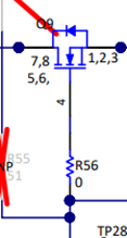
To calcualte the Switch timings i search for additional information for the internal high side driver.

Inside the pin equivalent diagram the internal fets to switch "ON" the FETs aer shown. What is the resitance value of this drivers.

What is the minimum series (gate) resitance in sereis to the CHG and DSG pin to drive the FETs? Can I place 0R without damaging the BQ chip?

I know fast switching has other issues but i would like to understand the maximum possible what can be provided by the BQ chip.

Thanks

BR

  • Hello Max,

    The pin equivalent diagram shows a simplified circuit of the internals in which we do not have characterized to share.

    You should be fine with placing a 0R in series to the DSG/CHG pin as shown in Figure 5-11. Schematic Diagram FETs in the BQ76952EVM User’s Guide.

    Section 16.5 FET Driver Turn-Off in the datasheet and Section 6 CHG Driver and Section 8 DSG Driver from this app note should also be helpful for more information regarding the FETs Driver.

    Best Regards,
    Alexis

  • From Figure 5-11 of the Schematic Diagramm in the BQ76952EVM ther is always at least a 5.1k resitor in series from the DSG and CHG Pins (not 0R). Therfore i do not understand your feedback, please explain more detailed.

    The Section 16.5 only showing FET driver turn off, but nothing about turn on. Also no valid source of inofrmation.

    In the app note "multiple FETs" there is a measurement for different switch ON characteristics. The minium used/shown is 100R but not below that vaule. Is this the limit?

    Would be great if you can provide me additional feedback to see what is the limit of the BQ in terms of small sereis resistance and what are the internal resistancves of the DSG and CHG pins.

    Thanks

  • Hello Max,

    Apologies for the confusion. The gate resistance being 0 Ohms was referring to R56 as shown below in the EVM schematic. 


    In the app note "multiple FETs" there is a measurement for different switch ON characteristics. The minium used/shown is 100R but not below that vaule. Is this the limit?

    The pin resistor is not recommended below 100 ohms to provide isolation for the pin from the current path.

    Best Regards,
    Alexis