This thread has been locked.

If you have a related question, please click the "Ask a related question" button in the top right corner. The newly created question will be automatically linked to this question.

LM5177: Schematic review

Part Number: LM5177
Other Parts Discussed in Thread: CSD17318Q2

Tool/software:

Hello,

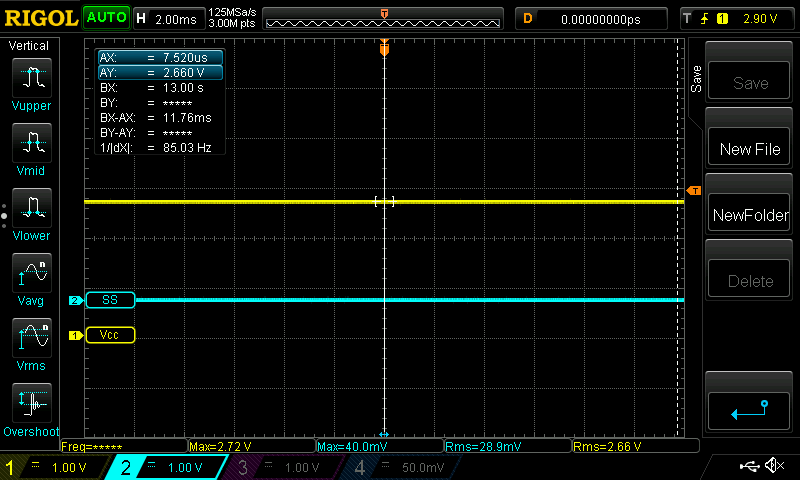
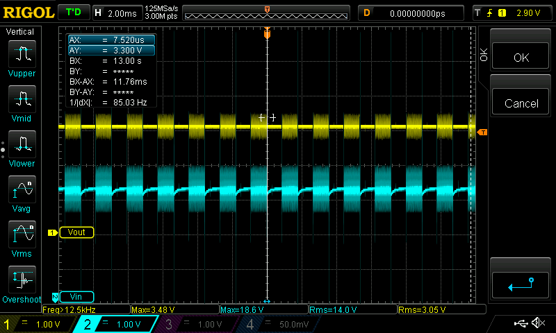
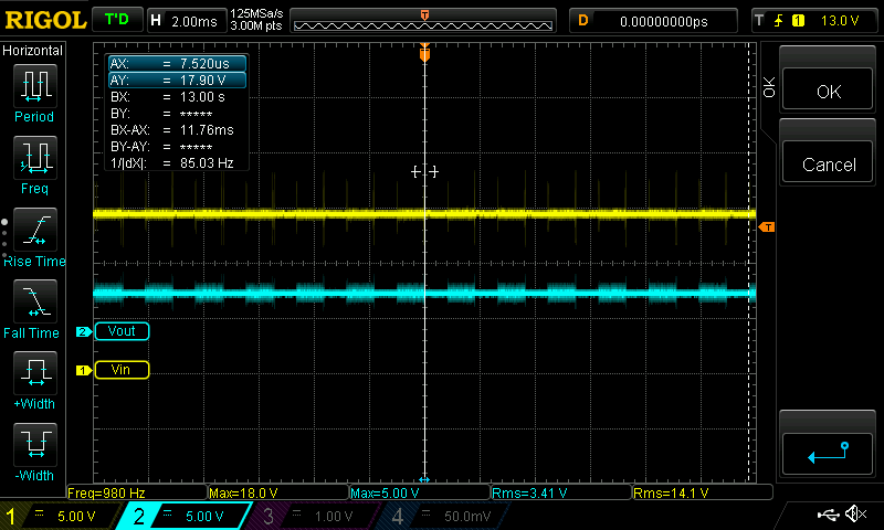
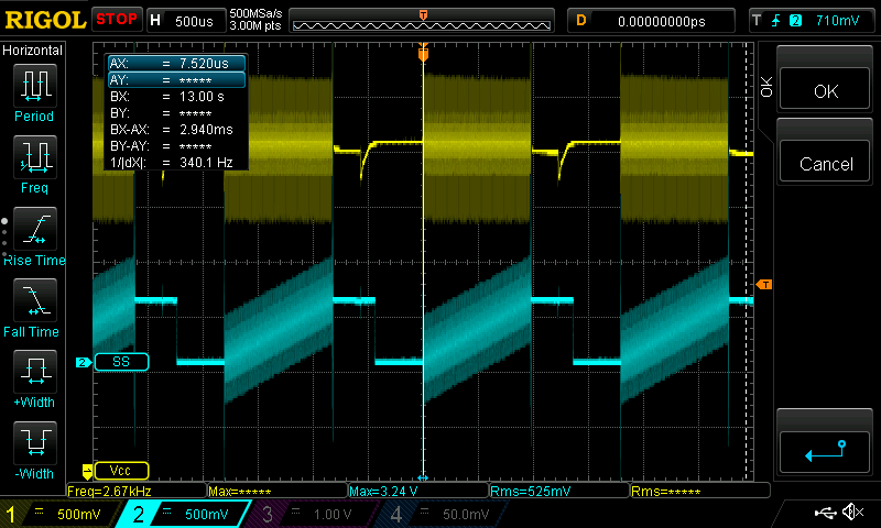
I have used the Webench tool and reference documentation to develop the following schematic. The design is intended to operate with an input voltage range of 10.7V to 40V and provide a regulated 12V output. The key configuration parameters are as follows:

  • Mode of Operation: AutoMode
  • Spread Spectrum: Disabled
  • Hiccup Mode: Enabled
  • uSleep: Enabled
  • IMON Limiter: Disabled
  • Monitoring Fault Indication Pin: Disabled
  • Output Current Monitor: Disabled

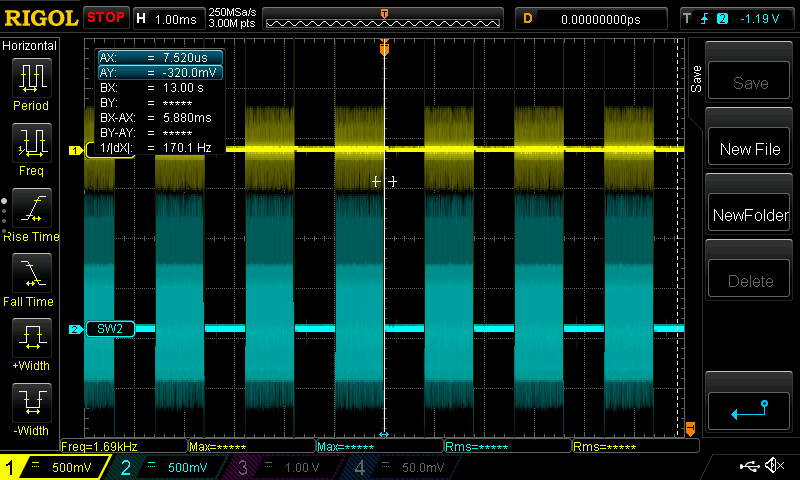
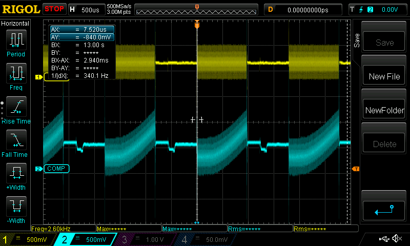
However, after prototyping the circuit, the output voltage is only 2.4V. I would appreciate any insights or feedback on potential design issues that could be causing this behavior.

  • Hi Connor,

    with an initial review of the schematic I could not see an issue.

    Can you probe following signals ( each showing a few cycles of f_SW and ~ 10ms):

    - VIN / VOUT

    - VCC / SS

    - SW1 / SW1

    - FB / COMP

    Best regards,

     Stefan

  • Thank you for the response, here are the requested signals.

    It appears there is no output when Vin is less than 14V and after increasing Vin to 16V there is no longer any output at all. This means that after increasing Vin to 16V SS, SW1, SW2, Vout, FB and COMP are all now 0V. Unfortunately I did not get measurements for SS, SW1, SW2, FB, or COMP before this occurred. Note Vcc remained at a steady 2.66V even after the other outputs died.

    Vcc/SS

    Vin/Vout

  • Hi Conner,

    the controller does not start below ~13V due to your setting of the UVLO (so this is expected).

    As the VCC does only reach ~ 2.6V this does indicate that the controller got damaged and you need to replace it.

    Such a damage typically happens due to large undershoot on SW1 and/or SW2. So you should check this signals carefully once you have the boards working again.

    This undershoot can lead to and overcharge of the Boot Caps above the abs max ratings shown in the datasheet which then can lead to a damage of the VCC LDO or the structure around that.

    Best regards,

     Stefan

  • Hello,
    After replacing the controller here are the requested waveforms:

    Vin/Vout:

    Vcc/SS:

    SW1/SW2:

    FB/COMP:

  • Hi Connor,

    I assume you have a lot of noise pickup here - this could be due to the probe setup.

    Esp the second plot VCC and SS make only sense with that assumption. So think you see the switching noise in all this plots.

    Can you please check your probe and also the ground connection and finally the length of the GND connection of the probe used (should be as short as possible).

    What you also can see in this plot that the SS pin ramps up to ~ 700mV and then stops. SS is finished at 1V so before reaching the target output voltage the controller detects an error - most properly an overcurrent - and then restarts.

    In this case either you load is to high, the softstart time to short ( also need to consider the inrush current into the output caps), or the noise pick up of the peak inductor current sense (CSA/CSB) is to high.

    Note: your Filter on CSA/CSB does not follow the recommendation in the datasheet. Also check if you have routed the CSA/CSB lines as kelvin connection between the sense resistor an the LM5177 - do not share this line with SW1

    See also: 

    Layout Optimization of 4-Switch Buck-Boost Converters

    Best regards,

     Stefan

  • Hello,

    The issue does appear to be due to the CSA/CSB lines not being kelvin connections between the sense resistor and the LM5177. After correcting this, the controller no longer restarts. However, the SW1 line now exhibits rapid overshoot oscillations, quickly damaging the controller. Could this be due to incorrect MOSFET selection, or is it more likely a layout-related issue?

  • Hi Conner,

    all can have here an impact.

    This overshoot or undershoots are mainly driver by parasitic on the boards and components.
    Most important is here to have a good layout - see the previous recommended app note but also here you can find a lot of additional info:

    (1) Four-switch buck-boost layout tip No. 1: identifying the critical parts for layout

    (2) Four-switch buck-boost layout tip No. 2: optimizing hot loops in the power stage

    (3) Four-switch buck-boost layout tip No. 3: separating differential sense lines from power planes

    (4) Four-switch buck-boost layout tip No. 4: routing gate-drive and return paths

    Also with adding gate resistors and/or snubber to the switch node you can prevent or limit this overshoots.

    But based on your layout you have already placed them and also the values does not look to bad.

    So in this case i would recommend to review the layout first and esp. take care about the current loops of:

    - gate line (esp. consider the return path of the high side MOSFET is the SWx line)

    - power stage, e.g. are the input and output caps close to the MOSFETs, is there a good Ground connection, ...

    For the MOSFETs you have selected: also this are not the best for this controller. The LM5177 does control the Gate lines with 5V and the selected MSOFET at 5V just go into the full conduction mode, so there is not a lot of margin. Also this could have an impact on the SW ringing.

    Best regards,

     Stefan

  • an additional note:

    the csd17318q2 (Boost side MOSFET) is here better then the CSD18514 (BUCK side MOSFET)

    Best regards,

     Stefan