This thread has been locked.

If you have a related question, please click the "Ask a related question" button in the top right corner. The newly created question will be automatically linked to this question.

LMR33620: UVLO Calculation for Negative Power Supply Design with LMR33620

Guru 12155 points
Other Parts Discussed in Thread: LMR33620, LMR33640

Hi,

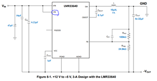
We are designing a negative power supply using the TI LMR33620 and are implementing external UVLO as described in the datasheet. However, we have some concerns regarding the applicability of the UVLO resistor calculation formula provided in the documentation.

Our Understanding & Concerns:

  1. Applicability of the Existing UVLO Calculation for Negative Power Supply

    • The formula given in the datasheet appears to be designed for positive power supply configurations.
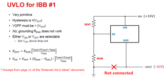
    • In our negative power supply design:VIN = 16V, VON = 15V, RENB = 10kΩ, VEN-H = 1.231V, Vout = -16V
    • We are concerned whether the existing formula can be directly applied to a negative power rail.
  2. Modified UVLO Calculation for Negative Power Supply

    • Based on our understanding, the calculation should account for the absolute values of V_ON and V_EN-H to ensure proper resistor divider operation.
    • We derived the following modified formula for negative voltage UVLO: 
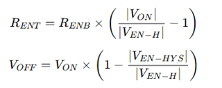
    • Could you confirm if this adjustment is correct for a negative power supply application?
  • Can the UVLO resistor calculation from the datasheet be directly applied to negative power supply designs?
  • If not, could you provide the correct formula or recommended approach for UVLO configuration in a negative voltage system?

Thanks,

Conor

  • Hello

    The equations in the data sheet would not apply to the IBB.

    Adding UVLO to the IBB is a little tricky.

    I have attached a document that should help you with your UVLO calculations.

    Please provide more details about what you wish to achieve and we can discuss further.

    Thanks

    UVLO_ideas_revB2.pptx

  • Hi Frank,

    I would like to delay the output timing of "-VOUT" relative to "VIN." Do you have any recommendations or suggested circuit configurations to achieve this?

    Under our current conditions, the recommended input voltage range for the enable pin is -16V to 0V. Given this, I believe the circuit configuration shown below is not recommended, correct? On our custom board, RENB is connected to the board’s GND (0V) as illustrated in the diagram below.

    We have confirmed through experiments that adjusting the resistance values of RENT and RENB allows us to delay the "-VOUT" output. However, we would appreciate your expert advice on whether this approach is appropriate and if there are better alternatives.

    Thanks,

    Conor

  • Hello

    I think that any of the suggestions for IBB in the document I provided should work.

    Connecting RENB to -Vout is the correct configuration.

    Thanks

  • Hi Frank,

    Let me confirm one thing. Here is my understanding of IBB.

    ---
    Because the voltage of the EN pin is determined by the voltage division between +16V and GND, a positive voltage of 0V or higher is applied to the EN terminal in the circuit configuration in the previous post.

    If VIN is +16V and VOUT is -16V, the recommended input voltage range for the EN pin is -16V to 0V.

    This is because in the Inverting Buck-Boost (IBB) configuration, the GND terminal of the IC is connected to -VOUT (-16V), so the reference potential of the IC is -16V.

    As a result, the voltage of the EN pin must also be kept within an appropriate range (-16V to 0V) for this reference.

    On the other hand, if a voltage of 0V or higher is applied to the EN pin, it will deviate from the recommended operating range of the IC, and there is a risk that the operation will become unstable or the IC will be damaged.

    --------

    However, in the following document, the EN terminal is directly connected to VIN. In this case, I think it is outside the recommended input voltage range for the EN pin.

    Is this design acceptable?

    https://www.ti.com/lit/an/snva856b/snva856b.pdf

    Thanks,

    Conor

  • Hello

    The important voltage ratings are specified between a pin and the PGND/AGND pin of the regulator.

    For both the LMR33640 and the LMR33620 the maximum allowable voltage between the EN pin and PGND/AGND is 38V.

    While the maximum recommended voltage is 36V.  So, in figure 8-1 that you show from the document, the voltage between EN and 

    PGND/AGND is 12V+5V = 17V.  That is safe.

    In your case, if you connected the EN pin to the VIN pin, the voltage between the EN pin and the AGND/PGND would be 16V+16V = 32V.

    That is safe.

    Thanks

  • Hello

    I will close this due to inactivity.

    Thanks