Tool/software:
Hi Sir,
we can know that out of 9 PCBs tested, only 1 can have output and pass? as attached below,
and since we don't know the reason, could help us check if the schematic is correct?
Tool/software:
Hi Sir,
we can know that out of 9 PCBs tested, only 1 can have output and pass? as attached below,
and since we don't know the reason, could help us check if the schematic is correct?

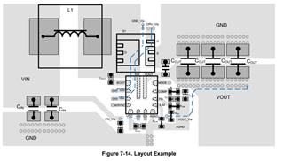
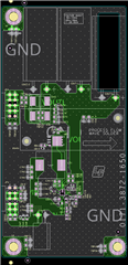 Hi Fergus, here is our Layout brd file ,please check the file, thanks