Tool/software:
Hello,
I am testing the TPS55288RPMR on a small prototype board before integrating it into my design. I would like to use the chip solely as a boost converter, so I have not connected the buck control pins. Is this a viable approach?
My application is for charging a battery, where an external MCU will control the charging process. The input voltage is currently set to 5V for testing, and I need an output of 14V at a maximum of 10A. My goal is to configure the device via I²C.
I am currently testing with an Arduino and can successfully communicate with the chip via I²C. I can configure all the registers without issues. I leave all registers at their default values except for MODE, which I set to 1 to enable I2CADD at 1, setting the I²C address to 0x75. This part works correctly, and the values are stored properly.
However, when I set OE (Output Enable) to 1, the chip seems to reset, and all registers return to their default values. At no point have I managed to get the device to switch—it only outputs Vin minus the diode drop.
To ensure correct register writing, I performed a sequence where I first read all registers, then wrote to the MODE register (setting OE, I2CADD, and MODE), and finally read all registers again. Here are the results:
Initial Register Read:
REF (L) (0x0): 0xD2
REF (H) (0x1): 0x0
IOUT_LIMIT (0x2): 0xE4
VOUT_SR (0x3): 0x1
VOUT_FS (0x4): 0x3
CDC (0x5): 0xE0
MODE (0x6): 0x20
STATUS (0x7): 0x1
Writing to Register 0x6 (MODE) - Setting OE, I2CADD, and MODE
Register Read After Writing MODE:
REF (L) (0x0): 0xD2
REF (H) (0x1): 0x0
IOUT_LIMIT (0x2): 0xE4
VOUT_SR (0x3): 0x1
VOUT_FS (0x4): 0x3
CDC (0x5): 0xE0
MODE (0x6): 0x20
STATUS (0x7): 0x1
I have tested this on two different boards, and I obtain the same results in both cases.
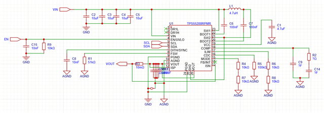
I have attached the schematic in case you would like to review it.
I would appreciate any insights into why the registers reset when enabling OE and why the chip does not start switching.
Thank you!