Tool/software:
Hi Mike,
I am proceeding with a design based on the application note SLUA560D: "UCC28950 600W Phase Shifted Full Bridge Design Review/Application Report (Rev. D)", and I have encountered several questions where the formulas and calculation results appear to be inconsistent. These include topics that have been discussed in related threads to date, but I would appreciate clarification on the following points:
Q1. Regarding Formula (11) in SLUA560D
Shouldn't the denominator of Formula (11) be "/2" instead of "/4"?
According to Formula (31) in the datasheet SLUSDB2B, the denominator is "/2", which would give a result of 50A. Could you confirm which is correct?
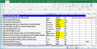
Q2. Regarding Formula (61)
Based on Formula (61), VdsQE should be 39V, but in the diagram you previously provided, it is shown as 19.5V.
Could you explain how 19.5V was calculated?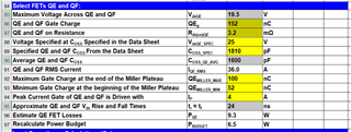
Q3. Regarding Coss_qe_avg in the diagram
In the diagram mentioned in Q2, Coss_qe_avg is shown as 2262.07 pF.
I believe this value may have been calculated using Formula (64) where the numerator and denominator are reversed incorrectly.
Could you kindly verify this calculation?
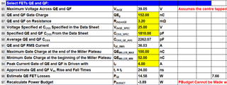
Q4. Regarding PBUDGET calculation error
When I perform an automatic calculation using the parameters provided in the application note, PBUDGET becomes negative, and an error occurs.
Therefore, I suspect that there may be a mistake either in the application note itself or in the provided Excel design tool.
Could you please check this issue in detail?
Q5. Regarding SYNC Pin Handling (SLUSDB2B Datasheet)
In the datasheet SLUSDB2B, there are two different recommendations regarding how to handle Pin 16 (SYNC) when the synchronization function is not used:
- In Section 6.3.15 (Synchronization SYNC):
"If the synchronization feature is not used, then the SYNC pin may be left floating, but connecting the SYNC pin to GND through a 10kΩ resistor will reduce noise pickup and switching frequency jitter."
- In Section 7.4.1 (Layout Guidelines):
"For the SYNC pin: this pin is essentially a digital I/O port. If it is unused, then it may be left open circuit or tied to ground through a 1kΩ resistor."
Could you clarify whether either 1kΩ or 10kΩ to GND is acceptable?
Best regards,
Conor