This thread has been locked.

If you have a related question, please click the "Ask a related question" button in the top right corner. The newly created question will be automatically linked to this question.

TPS53681: Adjustment of parameters

Part Number: TPS53681
Other Parts Discussed in Thread: CSD95490Q5MC,

Tool/software:

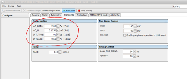
I design power supply system(TPS53681 & CSD95490Q5MC) for FPGA(XCZU67DR).
I am using Fution digital power designer.
But I don't know how to adjust compensation parameter.
How can I adjustment these parameter?

  • Hi Kenji Shimada,

    These are the control loop parameters (in simple terms proportional and integrator gains). These depend on what your system requirements are.

    In order to help you tune these parameters, I need to know your system requirements like number of phases of operation, output voltage, switching frequency, inductor value and output capacitor value.

    Thank you,

    Ashwin K

  • Thank you for your support.
    Following is system requirement.
     

    number of phases of operation = 2

    output voltage                           = 0.850V

    switching frequency                  = 500kHz

    inductor value                           = 560 nH

    output capacitor value              = 1320 uF/phase

  • I use one more power rail(rail#2).
    Following is following requirement.
    please support this requirement too.

    number of phases of operation = 1

    output voltage                           = 0.850V

    switching frequency                  = 500kHz

    inductor value                           = 2.00 uH

    output capacitor value              = 1320 uF/phase

  • Now I can't start up power supply rail#1 & rail#2.

    So please teach me the trouble cause.
    I send problem_issue.pdf & parameter.xml file

    TPS53681 @ PMBus Address 105d Project_050317b.xml

     I attached problem_issue.pdf 

  • Hi Kenji Shimada,

    Before I look into the loop, I have few more questions.

    1. When you say its not powering-up, are you getting any fault? If yes - what fault and can you please share a waveform with atleast one CSP, one PWM, TAO/TSEN and VOUT ?

    2. Do you have any transient spec to meet ?

    Thank you,

    Ashwin K

  • I mesure waveform.
    Please see this pdf2086.Problem_issue.pdfThank you

  • Hi Kenji Shimada,

    Thanks for the waveform. I can see something weird happening to VOUT, but I need a better waveform to root cause it.

    Waveform needed: In a single waveform use 4- channels to probe VOUT, PWM1, IOUT1, TSEN during boot-up(when enable comes up) for both Rail 1 and 2. So I need just two waveforms. (Need to see what's happening to PWM and IOUT when the VOUT is jumping in that fashion)

    Another question:

    How are you giving the enable? Is it using a control PIN or software enable using Fusion tool? Is the control PIN tied to all the supplies like 3v3, 5V etc. ? If you are in control PIN, just repeat the experiment by using the operation ON/OFF command in Monitor tab in Fusion tool. (Change the On/Off config to operation and use the operation to turn it on once all the other supplies are already there.)

    Operation

    Thanks.

  • control pin is tied to 3.3V.
    I try software enable with Fution tool, but problem is no change.
    I attacched file

    1,problem_issue.pdf(waveform&circuit design)

    2, parameter.xml

    Please review1031.Problem_issue.pdf it.

  • I think this problem is caused by VOUT starting up in a staircase pattern as shown in the figure below. What do you think?

  • Hi Kenji Shimada,

    After looking at the waveforms I suspect the following:

    1. For Rail 1, it is clearly a case of DCM operation. In your config file, you can change the DCM configuration to CCM in 1-Ph. 'Store to NVM' and repeat the experiment. 

    2. For rail 2, it looks like loop instability issue. You have to tune the loop parameters based on the compensation parameters. Right now it looks like all your parameters are high which makes the loop bandwidth very high and phase margin very less because of which you see a lot of ringing in the system.

    Following are the steps you can follow to tune the loop:

    a. As a starting point, you can keep ACLL as 0.5mohm, INT_TIME as 5us and AC GAIN as 0.5 to start with and try wake up.

    b. In order to increase bandwidth (make loop faster but start seeing some oscillations at higher bnadwidth) - increase AC GAIN or decrease ACLL or decrease INT_TIME or increase INT_GAIN.

    c. Vary these parameters individually first to set to your desired point.

    Please let me know of the results.

    Thanks.