This thread has been locked.

If you have a related question, please click the "Ask a related question" button in the top right corner. The newly created question will be automatically linked to this question.

BQ34Z100-G1: BQ34Z100-G1 pins details (VEN & TS/P6)

Part Number: BQ34Z100-G1
Other Parts Discussed in Thread: BQ34Z100

Tool/software:

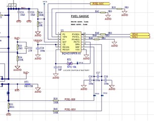
What are the exact electrical characteristics of pins VEN and P6/TS?

I couldn't find sufficiently detailed information in the data sheet.

  1. What are electrical properties of VEN? It would be good to know at least the following:
    1. If it is an open-drain output, how much current it can sink?
    2. Does it incorporates a current limiting function?
  2. The pin P6/TS is described as input type in Table 5-1 and also in the functional block diagram (Section 7.2). However, Table 7-21 and description below it give different impression ("However, note that in LED/COM mode 2, pin TS/P6, which has a dual purpose as temperature sense pin, will be driven low except when temperature measurements are made each second." Similarly, Figure 8-4 seams to suggest that in some modes it is used as an output.
    1. Again, what are electrical properties of the pin TS/P6?
    2. Is it input only or is it an I/O?

More details please.

Goran

  • Hello Kesav,

    1a.) the ven is a open-drain output that can do -0.3V to 5.5V and doesn't have a current rating but consumes 45uA typically, assume a standard current rating a a GPIO pin
    1b.) It does not use current limiting function since this pin is not meant to carry any large loads

    2a.)There is no electrical properties public information on this pin due to it solely being use for either thermistor or as LED/COM mode 2
    2b.) This is considered to be a ADC channel for mainly thermistor measurments.

    Thank you,
    Alan  

  • Hello Alan,
    Answer 1a.) matches what the data sheet says, but it contradicts this: "The VEN pin is configured as as output and input all of the time. It will pulse to 2.5V every 1 second when the voltage measurements are taken. It also sinks current when pulled to 2.5V externally. " That is an explanation provided by TI here: https://e2e.ti.com/support/power-management-group/power-management/f/power-management-forum/296462/bq34z100-ven-pin-connection 

    We also noticed that the pin VEN produces 2.5V pulses when left open, i.e. matches what was stated in that link. Would such toggling between 0V and 2.5V be possible if it was a simple open-drain output? From what I observed, I would expect that there is some kind of internal bias on VEN pin.

    In our circuit this IC periodically sinks excessive current (via REGIN pin). Specifically, about 20mA every 1s for duration of 120ms. That is the reason why we are checking pins such as VEN, for which the data sheet suggests that they could be tied to GND if not used.

    Any additional thoughts to help us with troubleshooting?

    Kind regards
    Goran

  • Hello Kesav,

    I'll look into this and give a response within the week.

    Thank you,
    Alan

  • Hello Alan,
    Any progress with resolving this issue?
    Kind regards
    Goran

  • Hello Alan,

    I noticed that on our board pin REGIN (power supply input, i.e. input to internal LDO) occasionally sinks around 20mA (Tpulse=125ms, once every 1s). Which seems to be well above any value for ICC specified in the data sheet (145uA nominal (Table 6.3) & 10mA ICC(PROG) MAX (Table 6.12)).

    I suspected that current may be going to Vss (i.e. GND) via VEN pin (not used in our design), which was tied to Vss (as suggested in the data sheet).

    I inserted 11R resistor between VEN and Vss and checked voltage across it on a DSO - there was 220mV pulse (Tp=125ms, every 1s). That matches 20mA current pulse coming in via REGIN pin.

    That current pulse imposes about 2.5mA of average ICC current (well above 145uA value stated in Table 6.3). In our case, this may yield about 1.8Ah over 30 days in standby mode, which is too much for application.

    Would it be correct to conclude that VEN is not a simple open-drain (it appears more like a low side switch with an internal load (current source?). Otherwise, the chip seems to be working OK.

    1. Is such behavior expected?
    2. Would it be better to leave pin VEN floating? (In other words, should we be aware of any potential misbehavior if it is left floating?)
    3. Is there any other document that complements the data sheet with more detailed information about the pin characteristics?

    (I asked this question 20 days ago - it would be highly appreciated to get it resolved in next few days.)

    Kind regards
    Goran

  • Hello Kesav,

    To better address you issue could you send a schematic to validate that your schematic is done correctly. Also the behavior of going above 145uA does seem excess (depending on the firmware version there is different mode consumption but this is also dependent on application as well). It is best practice to leave VEN tied to Vss since false signals can come from EMI, ESD and etc. Lastly the most detailed document on pin characteristics is the datasheet and this is found on the product page.

    Thank you,
    Alan

  • Hello Alan,
    The schematic is attached.

    Few pointers:

    • VREGIN is connected to 3V3,
    • R36/R37 divider provides voltage feedback and
    • R31 is current sensing resistor.
    • SDA1 and SCL1 have pull up resistors to 3V3 on other side (not shown).

    The following contradicts data sheet: "It is best practice to leave VEN tied to Vss since false signals can come from EMI, ESD and etc. "

    Judging by Figures 8-3 & 8-4 in the data sheet, VEN is unlikely to be an open collector. Without some kind of internal pull-up, the gate of MOSFET Q4 would be floating in some states (e.g. when SW1 open & VEN off).

    Hopefully this will help to move closer to a resolution.

    Kind regards

    Goran 


  • Hello Goran,

    After consulting with my team, If the VEN pin is ground or left floating than your battery setup is a single cell however if you are doing multiple cells in series than you must use the VEN pin as a "Active High Voltage Translation Enable". For more clarification what is your battery setup, also if you are indeed using a single cell than you should not be seeing increase current consumption regardless if it is left floating or grounded.

    Thank you,
    Alan 

  • Hello Alan,

    I don't think the following is a correct interpretation of the data sheet: "if you are doing multiple cells in series than you must use the VEN pin as a "Active High Voltage Translation Enable". "

    According to the data sheet VEN pin can be used to switch on/off the voltage divider. In other words, isn't it an option, rather that it must be used?

    Furter, in designs that use it to enable the divider, wouldn't it only reduce power consumption of the divider, not of the IC?

    As I mentioned before, what we are seeing is 20mA pulse getting out from VEN pin into GND (in via REGIN pin). If the battery has 25V, how would you explain that current pulse of such magnitude in relation to the voltage divider (560K +20K)?

    One more thing, regarding:

    "if you are indeed using a single cell than you should not be seeing increase current consumption regardless if it is left floating or grounded".

    If VEN pin is left floating, is there a path for current to flow out of it?

    Kind regards
    Goran

  • Hello Kesav,

    According to the data sheet VEN pin can be used to switch on/off the voltage divider. In other words, isn't it an option, rather that it must be used?

    Furter, in designs that use it to enable the divider, wouldn't it only reduce power consumption of the divider, not of the IC?

    -Using the VEN pin is not a "must" when using multiple cells packs, rather it is heavily suggested due to increase current use with out using it. This is most likely the reasoning for your increase current use. The VEN pin is meant to save on current use 

    If VEN pin is left floating, is there a path for current to flow out of it?

    -If VEN pin is left floating it would be an open circuit meaning no current would flow out of it.

    Thank you,
    Alan

  • Hi Alan,

    After 3 weeks we are at the same point where we stared.

    You still haven't explained to me how VEN pin sources current if it is an open-drain output.

    Any chance that you repeat the same test I did and let me know the results?

    Kind regards
    Goran

    PS
    Maybe it is time to escalate this to the next level?

  • Hello Kesav,

    You still haven't explained to me how VEN pin sources current if it is an open-drain output.

    -Please review the first comment I made on this trend below 

    1a.) the ven is a open-drain output that can do -0.3V to 5.5V and doesn't have a current rating but consumes 45uA typically, assume a standard current rating a a GPIO pin

    If your issue is that your system is consuming too much current than implementing a VEN will reduce your power consumption within your system, and although it is not mandatory to use VEN with mutli-cell system it is heavily recommend. I can re-assign this trend to the product line expert as well.

    Thank you,
    Alan

  • Hello Alan,

    "I can re-assign this trend to the product line expert as well."

    Please do, I need to resolve this problem.

    BTW: Are you member of TI staff or you are just a member of the forum?

    Kind regards
    Goran

  • Hello Kesav,

    The BQ34z100 expert is currently out office but he would be able to answer your question. Please give some time before responding on the post.

    Thank you,
    Alan

  • Hi Goran,

    The VEN pin is used to control the FET Q4 on our EVM, this FET turns the voltage divider on and off. When this pin is not used, current consumption will be increased because the voltage divider cannot be turned on and off and will remain on. The VEN pin is not required but if it is not used current consumption will be increased. Other factors such as the FW you are running can affect the current consumption in different power modes.

    Not sure if this fully answers your questions the above thread was convoluted. Please let us know if there are any more pending questions. 

    Regards,

    Diego

  • Hi Diego,

    That is obvious from the data sheet and does not answer my question (and has been already refused as a plausible answer in the previous replies).

    As you can see from our schematics we do not use VEN pin to drive voltage divider and VEN is tied to VSS, via R50 (0R0, so effectively short connected to VSS as suggested in the data sheet).

    As our battery voltage is 24V, current trough voltage divider (connected to pin BAT) can't be more than 24V/(560k+20k)=42uA or in the worst case 24V/560k=43uA. In addition, that current comes directly from the battery, not via REGIN. So, that eliminates the voltage divider as a culprit considering excessive current pulses of 20mA.

    In our tests, we found excessive pulsing current entering REGIN pin from an external 3V3 linear regulator, to which it is connected. (To avoid any misinterpretation, that is the current that goes into REGIN pin only, not a current from the regulator that may be shared with some other loads - it solely goes into REGIN pin).

    In the data sheet I found that the typical supply current in normal mode is Icc=145uA, while max Icc is for flash memory write mode, specifically Iccprog(max)=10mA.

    We are seeing a periodic current pulse (peak 20mA, with duration of 125ms) all the time. Simple comparison of observed 20mA vs the stated 10mA suggested that it may not be caused by the flash memory write mode, so I continued the investigation.

    What I found is that the current pulse that enters into BQ34Z100PWR-G1 device via REGIN pin, exists via VEN pin - approximately 20mA peak on both pins. To me, it suggests that no other pins contribute to the observed current pulse (e.g. nothing to do with the voltage divider connected to BAT pin nor VEN being an open drain).

    Here is how I tested VEN pin. The original R50=0R0 was substituted with 11R resistor and voltage drop across it was  observed by a DSO. Clearly there was 220mV pulse (Tp=125ms, every 1s initially, then after some time every 20s), which corresponds to 20mA pulse going from VEN into VSS.

    I couldn't find anything about this pulse in the data sheet and have two simple questions:

    1. Is the observed behavior normal?

    2. What are electrical properties of VEN?

    Among other things, your colleague suggested that it is an open drain output, which is hard to believe for the following two simple reasons:

    • If it is an open drain (ref. to VSS), it couldn't source 20mA. (If it is ref to VDD, obviously the data sheet suggestion to tie it to VSS when not used would be totally wrong.)
    • Considering the schematic of your evaluation board (Figure 8-4 in the data sheet), if VEN is an open drain output, wouldn't gate of Q4 be left floating whenever VEN is off (in Hi-Z state)? In other words, would the gate of MOSFET Q4 be left without bias? (I don't believe so.)

    (From the perspective of what I have observed, why should I accept suggestions such as that the issue is caused by the voltage divider or that VEN is an open drain? After frustrating 4 weeks of going around in circles in this forum, I expect to get a plausible answer soon.)

    Kind regards
    Goran

  • Hi Goran,

    Is the observed behavior normal?

    It is normal for the current consumed to fluctuate. The current consumption is specked over a period of time; the gauge will draw more current at time depended on many factors such as what operating mode the gauge is in, what the gauging is doing, and what FW version is on the gauge. 

    With that being said on my set up I have never seen the gauge consume 20mA of current, even for a short pulse. I am using the EVM.

    From my personal experience, when customers use an external voltage divider and they use the VEN pin. I believe the issue is that you have voltsel set to external causing the VEN pin to pulse. If you switch voltsel to internal, I think the 20mA pulses may disappear, but your voltage divider ratio will be wrong, resulting in your voltage reading being wrong.

    What are electrical properties of VEN?

    I agree, I believe this a documentation error. 

    The VEN pin is configured as as output and input all of the time. It will pulse to 2.5V every 1 second when the voltage measurements are taken. It also sinks current when pulled to 2.5V externally.

    Regards,

    Diego

  • Hi Diego,

    Thanks for your reply, it is helpful.

    However, there are few more questions. (Sorry to ask such basic questions, but the data sheet seems to have some errors.)

    With that being said on my set up I have never seen the gauge consume 20mA of current, even for a short pulse. I am using the EVM.

    VEN is not connected to GND (Vss) on the EVM - could that be the reason? If you connect it to GND (Vss) what happens, does current go up?

    In our design VEN is not used and we connected it to GND (Vss), as suggested in the data sheet. Any potential issues if we do it differently, for example:

    1. Connect VEN to GND (Vss) through a pull-down resistor (say 1k-10k)?
    2. Leave VEN unconnected?
    3. Connect VEN to Vdd (REGIN) directly or via a pull-up resistor (say 1k-10k)?

    For us better options would be the pull-down resistor or unconnected, as in those two cases we don't need to go through redesign of our PCB layout.


    Kind regards
    Goran

  • Hi Goran,

    I can run these tests on my EVM and share the results, please allow me some time to get these test completed.

    Regards,

    Diego

  • Hi Goran,

    Testing on my side, my evm current pulses to around 32uA.

    connecting VEN to REGIN, significantly increased the current consumed by the device (~2ma).

    GNDing VEN slightly increased the current consumed (~45uA when pulsing).

    Regards,

    Diego

  • Hi Diego,

    That helps, just tell me if those values are RMS or peak?
    Regards
    Goran

  • Hi Goran,

    RMS

    Regards,

    Diego

  • RMS

    Could you see a 20mA pulse with duration of 125ms (rep rate 0.05Hz) when measuring RMS current?

  • Hello Kesav,

    I will be rerunning the test and will report the result when possible. Please expect around mid next week for results.

    Thank you,
    Alan

  • Hello Kesav,

    Update, pushing into starting the test to validate results soon. Trying my best to work through the duties of the role to dedicate time to this e2e.

    Thank you,
    Alan

  • Hi Alan,

    Considering that you haven't responded for a month, may I ask to escalate this issue to the next level - we need it to be resolved.

    We asked TI for help 3 months ago and we still have no answer to the specific issue we are facing, it is disappointing.

    Kind regards
    Goran

  • Hello Kesav,

    I have set aside time for Friday to perform the test, sorry for the delays this may have caused. Please expect a response by eod of day.

    Thank you,
    Alan

  • Hello Kesav,

    The unit during testing the EVM experienced a failure and no longer functional and a new unit is currently being sourced.

    Thank you,
    Alan