This thread has been locked.

If you have a related question, please click the "Ask a related question" button in the top right corner. The newly created question will be automatically linked to this question.

TPS40210: Boost won't start with a small load ot swing with small load

Part Number: TPS40210


Tool/software:

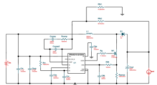
i created a classic boost for nixie, the first version was with poor perfomance, also i redign it and put bigger mosfet and bigger inductor:

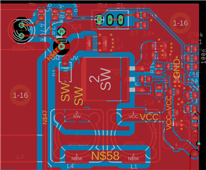
rerouted ground with as much as possible short ways:

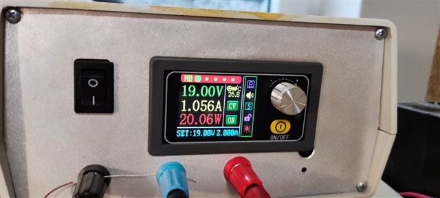
Input voltage : 12-19, output voltage 120-200v, 50-80mA, main MOSFET :

STB33N60M2, Mosfet, 600V, 26A, 190W,100mOm :  https://www.st.com/en/power-transistors/stb33n60m2.html

Working frequncy 78KHz

but now it is work only without load, with 2.5-3W laod it stop working and still restart

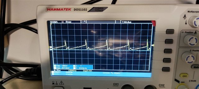
this is voltage on current sense :

this is voltage on power supply VCC :


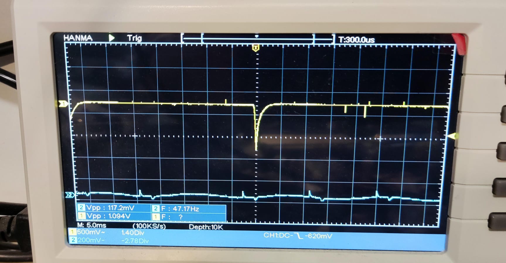
but i habe connected 20uF C8, and add 680uF direct over C8


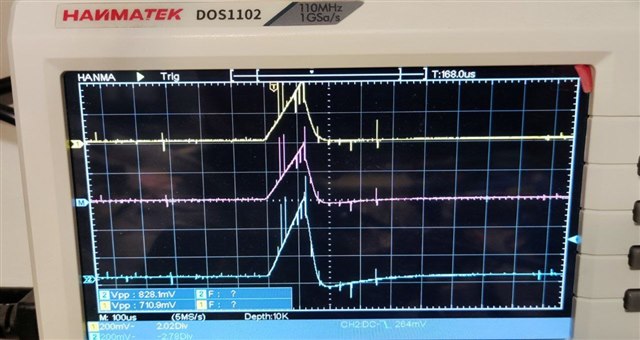
This is how it look on gate of MOSFET:

and this is source:

As i sad - this is only 2.5W load, without load it work, main coil will bu NOT saturted, i replaced it with big one, 350uH, up to 9A :

  • Hello I R,

    Thanks for using the e2e forum and adding all this information.
    I will review the design and will get back to you by tomorrow.

    Best regards,
    Niklas

  • Hi I R,

    Thanks for your patience.
    I am confused by the Isense signal.
    Not only does it rise to 600mV, which would mean peak currents of 12A, it also does not trigger the OCP earlier, which should be at 150mV.

    When you measuring with load, do you start up without load and then increase the load, or do you directly start up with load?
    The circuit might not be able to ramp up the output voltage and already supply the load at the same time without triggering the overcurrent protection.

    Best regards,
    Niklas

  • i try to meause current with two scope channels to calculate true difference, but get nearly the same result:

    the boost start from begin without any load with this short pack of pulses, for few seconds, pulses will be shorter and weaker and after 1-2 second i have setted voltage

    with 2.5w load it won't start and stay in "pulse" mode, now it the Rsense only 25mOm, or i try to short it fully, but still same behavior Disappointed

  • Hi I R,

    Removing the Rsense completely is not a possible solution, as the resistor is required for the peak current control regulation.
    The only option is to further reduce the resistance to avoid triggering the overcurrent protection, but I would only do this once we confirmed that the OCP is the root cause for the failure with 2.5W load.

    The measurements you show are from the ISNS pin of the IC, or from somewhere else?

    Best regards,
    Niklas

  • Removing the Rsense was just a test ...
    yes, i solder i wire to low side of Rsense, and chekk voltage on upper side and on ISNS pin, both the same, and i don't understand why, what is the problem with my layout

  • Hi I R,

    I recall you already shared the initial design in another thread some time ago.
    There are still some suggestions I commented that were not implemented in the newest revision, especially the ground loop of the input side, where all current will traverse directly below the sensitive IC on the ground plane back to the input caps.
    However, I do not know if this is causing the failure we see.
    The rest of the layout changes have been implemented and look okay to me.

    As mentioned in my previous message, the current sense measurement just looks unrealistic to me.
    The amplitude goes up to >400mV and it looks like one single 100% duty cycle pulse, so I assume the resolution is just very low.
    The MOSFET measurement shows that the device is indeed switch normally for several cycles, before it stops switching due to an unknown reason. (We discussed about OCP here)

    You confirmed the board is working okay without load.
    - Is it possible for you to start up the board with 0 load, and then increase the load during operation? -> This will confirm if the problem is the inrush current at startup
    - You reduce the sense resistance for 25mOhm, creating a current sense limit of 6.4A. Do you have the possibility to measure the inductor current, or do you only have voltage probes available in your lab?

    Best regards,
    Niklas

  • ok, i try to fix it again, but still have no luck

    without loat it start very slow with a lot of shut dows cycles like described above, after few second shutdowns will be shorter and shorter and it start ... only after 4-6 second it start working properly without load

    yes, spike with over 0.5v will be measured direct on TPS pin 7 - ISNS, all Rsense, and etc GND pins are "nailed" on back GND plane with ~20 vias, this few uOhm resistande and few nH inductance

    i can not undestand, what is wrong on PCB desigt, path from source of mosfet to sence resiator is 2mm, from sense to ground of IC - 4-5mm, frequency only 78KHz .. i solder derect on Rsense two wires and measure voltage with spring on oscilloscope probe direct on this two wires ... if i short just for test theis Rsence to zero - i have same behavior -> some other problem are on the board, but i have no idea what, why it is so buggy....

    no, i can not measure coil current


    this is how i measure voltage on pin 7, spring direct on ground Rsense and spike on RC connection bevore pin 7


    this is result

    one more weird behavior - if i go under 6v - boost go into "short cicruit mode", it stop working and draw 2+A

  • Hi IR,

    It is a bank holiday today. Please expect a reply by Tuesday.

    Best Regards,
    Feng

  • Hi I R,

    So even without load, the device is running into OCP for several seconds before it can achieve the target output voltage.
    If the issue is the same even if Rsense is shorted, the sensing signal might not be sensed correctly.
    Do you know the value for C6? The schematic just says 250. Is this 250pF?

    My general concern is that the device cannot support the large boost ratio. Especially if VIN drops down to 6V, achieve 200V output voltage may not be feasible with this design.
    The device should not have a 100% duty cycle mode, where it shorts the supply voltage. This "short circuit mode" feels like the application is failing.

    Best regards,
    Niklas

  • Hello Niklas,

    thank you very much for your patience,
    yes, it is 250pf, just values for RC are different to set frequency from 250 down to 78KHz

    if voltage drop to 6v it stop to switching and open main MOSFET to short Vin ...

    The main proble is not a boot ratio, i have same problem if supply voltage is 20v istead of 12v, and in the past i build simply boost with verly old mc34063 from 9 to 250v without any problem, up to 7-8W at 250v with over 80-85% efficency, just with limitation of big minimum switching time of 34063, i can not handle power over 10w (from 12v to 200v/50ma, one stage) with resonable inductor size :

    https://vfdclock.jimdofree.com/2015/07/18/openhardware-10w-mc34063-based-high-voltage-power-supply-module-high-efficiency-small-size/
    28x33x15mm, 10W boost (12v > 200v/50ma, 82-85%), work very well and stable, build 20+ of them for nixie clock Smiley

    i will try last try to change layout, will post picture of PCB later ...

  • Hi I R,

    Thanks for the explanation.

    I am very sorry that the debugging was not successful so far.
    After checking the schematic several times, I cannot find the problem there.

    Next to reworking the layout, I can also recommend to check of the components on the board are still okay after all the soldering. (e.g. in the last picture C8 looks pretty worn out)
    Feel free to get back to us if you need a review of the newest PCB.

    Best regards,
    Niklas

  • last try ... before i order last PCB, this is new layout, GND between MOSFER and TPS is only one polygone

    no current under IC, VCC to IC is own wire, different from VCC to main inductor, blocket direct with some capacitors

    i hope here are no currets over wrone ways, only from main inductor > HV diode > HV capacitor back to ground backplane

  • Hi I R,

    Thanks for sharing the re-design.
    The new power stage arrangement looks good to me. The IC is now on a calm ground area away from the power stage.

    Three more things I want to point out:
    - The power stage components are still placed with thermal relief pads. You made traced to improve the connected, but there are still a lot of cut-outs, which I would recommend to remove.
    Especially on the switch node, input/output caps and sense resistors. I marked them with black lines.

    - Can you check if a via is placed at the BP cap ground? If not, please place a via here so the loop between BP pin and GND pin is short. (I also marked this with a black arrow)

    - The feedback trace between the upper voltage divider resistors and the FB pin is rather long. With two 470kOhm resistors, the signal becomes very noise sensitive. There are no power traces nearby, but the trace still traverses below VCC and several other device pins.
    The implementation of this pin was similar in the previous revision. Did you recall any problems with the FB pin being noisy?

    Best regards,
    Niklas

  • Thank you !
    yes, the BP is shorted to back plane with via and i can add more via and will fill all cut outs with copper

    FB line ... i have no idea how i can place it shorter, last time it was ok, at 180v i has around 50-100mv noise,
    i think the most of them from outside, like my buggy chinese Led tablelamp, or i can made divider with lower values, i can sarifice  up to 1mA(160-200mW) current without problem...

    ok, i hope in two week if pcb arived it will work .. or go back to two old school MC34063 boosts with x2 10W Smiley

  • Hi I R,

    I agree that replacing the FB circuit is difficult, but noise on the FB can indeed be a risk of instability.
    A compromise could be adding a footprint for a small capacitor in the pF range close to the FB pin. This should be feasible from layout side and can already help stabilizing the FB voltage.

    Best regards,
    Niklas


  • no, it don't work ...

    with 12v input - 4W, with 19v input - only ~6.5w is a limit, after 7w load (19v input, 175v/ 40+mA load) it go in overcurrent mode and switch off unitil SS capacitor discharge

    only positive - it start normal, without problem ...

  • Hi I R,

    I will get some more feedback from within our applications team to see if we missed any major problems within this design.
    Please allow me some additional time until beginning of next week to get back to you.

    Best regards,
    Niklas

  • Thank you !!

    I want just to undertsand - why my fisr worstes design was the stablest one Smiley
    it was just hot, becase i use MOSFET with high Rdson .. but jeach time if i made my layout better - it work worster Smiley


  • It look like a problem, it this case  the capacitor on Rsense is around 400pf, now i get from 12v a littel bit more, around 5.6W (consumption power) as limit, this signal it direct between low side of Rsense and pin 7 ... Very high frequncy impulse reset the current limit

    In this schematic : neonkev.com/.../

    Capacitor is set to 2200pF ! i will try more too, from 1000 to 2200pf ..  will see


    UPD:

    ok, no really better, Vin 19v, Cfilt - at end 2200pF, peak power 9.5W (6W at Vin 12v) before go in overcurrent shut down


    UPD2:
    i short Rsense with weird loop - nothing changess, still 6W maximum power at 12v with overcurrent shot down  :


    WHY ?? 

    UPD3:

    Blue - drain of MOSFET, yellow - voltage on Rsense


    UPD 4:

    Bevore shutdown gate signal will be instable, if i rise input voltage - it will be stable, but at more load - again instable


    voltage on Rsense, 50mv/div, 50mOhm, also current rise up to 1A, 15v Vin, slow rise load from 6w (all stabe) to 9W (cut off)


  • Hi I R,

    Thanks for all the additional tests and measurements.
    My colleague got back to me and asked which inductance is used at the moment.
    In one of the early comments, it was 350uH. Is this still the case?

    With some quick calculations using our power stage designer ( https://www.ti.com/tool/POWERSTAGE-DESIGNER ),
    they pointed out that the device will go into CCM quite early ( ~2.5W) and the duty cycle will go up to 94%, which might be more than the device can handle.
    This would explain why the device becomes unstable.

    To keep the duty cycle below 85% at 6W with 78kHz switching frequency, a maximum inductance of 100uH would be calculated. A peak inductor current of 1.2A is expected here.
    Do you have a 50uH or 100uH inductor available to test this?

    Thanks and best regards,
    Niklas

  • Hi Niklas,

    i found the main problem: https://e2e.ti.com/support/power-management-group/power-management/f/power-management-forum/87851/leading-edge-blanking-problem-with-the-tps40210

    This look like typical LEB problem, as first test i take first quick and dirty solution - 4.7pf + 470 ohm from drain to ISIN pin  ..

    AND  (drumming) ....

    ISIN pin signal : 

       no more wild and crazy swing

    Burn baby, burn ! (230v/40W lamp at 150v as test load)

    this is no limit more


    now i need to opitomise compensation network, two calculators from TI and 3 external webpages give mit 4 totally different vlaues for it. the same for inductor, all calcutaros and webpages give me values from 47 to 500uH for same Vi/out Smiley

     Now i have 7-8v saw tooth peaks at 180v/90mA output, i can not recognize if it is compensation, or leaving CCM or something others

    And may be you have correct calculation/expectation for LEB parametrs depen on frequency/voltage/inductivity/power/etc ?
    Layout possibility ? i don't know how i can place 4 more part and don't destroy GND layout. Any bettes solution/calculation ?

    Internal LEB of TPS is only 75ns fixed, in this case it look lite too short

  • Hi I R,

    Glad to hear you found the root cause for the problem.
    For calculating the compensation, we normally use the power stage designer tool as well https://www.ti.com/tool/POWERSTAGE-DESIGNER
    You will find all necessary parameters within the datasheet.

    For reducing the leading edge spikes, an RC filter from SW to GND as in your quick and dirty approach may already be enough.
    Unfortunately, I do not have any simpler solution than mentioned in the other e2e thread.

    I know the TPS40210 device got reworked in 2022 to run with newest process technology. All specs and datasheet parameters stayed untouched, but the old device may have wider variances to the typical values, especially when it comes to specs like LEB.
    Can you check the package if you already are using the new device material?
    The new material should come from RFAB.

    Best regards,
    Niklas

  • i can not really trust values of this tool ...
    if my divider is 94k/400 (relativ high current) it suggest me unrealistic  2M Rcomp, 11nF Ccomp and zero Cff


    If i use excel specially for this TPS40210 from TI page, suggested values are totally different  116K/470nF/86pf

    Wbut with this values it totally unstable, only 5W  Load and wild peeping

    For my divider 940k/4 - 1M/47n/10pF - totally unstable, Load only 4w, chage to 250k/100n/100pF - load over 15w, but peeeep

    WEBENCH, one more bunch of values, again totally different ...  :


    From 2 other sources with ready schematics i have two more set of values, already different


    what is the source ot truth ? How i can calculate realistic values for my case ?


  • Hi IR,

    The engineer is out of office today. Please expect a delayed reply.

    Best Regards,
    Feng

  • Hi I R,

    I am sorry to hear that every calculator gives different results and none of the proposed values seems to be working.

    I tend to recommend the power stage designer the most, as this tool comes with an application note that explains how the calculation works, so it is possible to double check the calculations by hand. ( /cfs-file/__key/communityserver-discussions-components-files/196/Loop-stablity-application-note.pdf )

    If the calculations do not work, the best solution would be to build the compensation via bench tests.
    The common approach would be to start with a very slow compensation, e.g. just a single 1nF cap at the COMP pin.
    Then you measure the bode stability and shape the bode curve by adding additional poles/zeros through the R and C component addition.

    Best regards,
    Niklas

  • this is too much theory in this paper, if you official (created by professional engineers)  calcurators/simulators delivery very differen and not working results .. how can i be sure that i will found better solution...

    ok, i try with values different values and try to get support grom chatgpt/grok, i reply with much better answerl like official datasheet/claculator .. now i have power up to 14W at output with values at end FULLY differen from datasheet, 470pf Ccomo, an 33k/100n RC ..but sometime i have troubles to start with load ...

    and i found no explanation for this HUGE difference from official data/values

  • Hi I R,

    I agree that the topic of compensation theory is very complex.
    You can never be sure if your solution is the best possible implementation, but through testing you can see if the system is stable enough for your design requirements.
    I cannot give an explanation why the recommended values from AI tools differ so much from our tools provided, simply because I do not know the equation that are there.

    However, it seems to be good news that the design can up with 14W after modifying the compensation.

    Best regards,
    Niklas