Tool/software:
Dear Team,
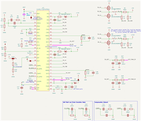
after we could resolve the "shoot through" issues by putting the LM5171 into Diode Emulation mode (DEM) using two resistors on the SS pins as described in the Datasheet, we now encounter the issue that the Channel 2 cannot boost nearly as much as channel 1.
Background:
Our LM5171 is employed to boost two different input voltages, namely 5V on CH1 and 3.3V on CH2 into a common 12Vout. We use a battery charged at 10.4 V as load for this test to maintain a fixed output voltage.
We use a 4 mOhm Current Sense shunt for both channels, overall both channels are designed to boost a maximum of around 10 A (The R_cs permits 12.5 A) and all components are selected as derived using the LM5171 Calculation sheet.
Channel 1 performs perfectly, we can boost up to 8-9 A input current to the output (more amps likely work too, we haven't tried yet, as we haven't hit a limit so far).
Channel 2 unfortunately doesn't allow us to boost more than 0.42 A. We have tried with different input (LV) power sources incl. an Ammeter in series to the input to quantify the 0.42A. We have tried raising the input voltage from 3.3V nom. to 5V to no relief, we have even tried soldering a R_cs in parallel to effectively halve its resistance in hopes to hit a limit at 0.84A and deduce a controller issue, but it still is fixed at 0.42A.
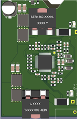
The Channel 2 is de facto completely symmetrical to Channel 1, as in reusing all passive components and a mirrored layout.
When wiring 3.3V to Channel 1, we can draw 2A+ (haven't tried higher), just to prove the point that something is off with Channel 2. (bottom channel in the layout picture). What could the issue be?
We currently only work with one prototype to validate the design. We would like to build around 50 PCBs employing LM5171 in this manner once we sorted out all issues.
Thanks for any insights or help