This thread has been locked.

If you have a related question, please click the "Ask a related question" button in the top right corner. The newly created question will be automatically linked to this question.

BQ79600-Q1: BQ79600, SPI_READY never triggers low

Part Number: BQ79600-Q1
Other Parts Discussed in Thread: BQ79616

Tool/software:

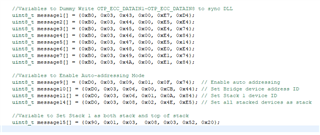
Hello! I am trying to use the BQ79600 and the BQ79616 to create a simple prototype. Our system has one stack device and one bridge device, but we are running into problems receiving the data back from the bridge device. We can see the serial communication between the bridge device and the stack device, and we can see the data being transferred, but SPI_READY never triggers back high after triggering low, so we never receive any data. I have attached an explanation document with Waveform photos and code photos. We are using the STM32 Cube IDE and the STMf042k6t7 microcontroller for our main microcontroller for the system..

WAVEFORMSHELP.docx

  • These arrays are what I send during auto addressing. I set the system up as one bridge device with one stack device with the one stack device being top of stack.

  • Hi Melena,

    I will look into the commands being send and will get back to you tomorrow.

    Thanks,

    Zachary

  • Hello, just wanted to follow up since its been a few days.

  • Hi Melana,

    Sorry for the delay. I wanted to speak with one of my colleagues who is more familiar to software on our devices, and he wasn't in last week. 

    I went through the data which you sent and there does seem to be an issue between MCU and base. I have a few questions so that I can debug this:

    1) This is being tested on EVMs? Are the EVMs configured correctly?

    2) Can you send me the logic files so I can take a look at them myself?

    3) If this isn't on an EVM can you send me the relevant schematic?

    4) Can you read the following registers from just the base device?

    Thank you,

    Zachary

  • Waveform Help.docxPrimaryPCBV2.pdfWaveform.csv

    Hello! Thank you for that! We did try to send the one read command, but we ran into the same problem where SPI_READY never triggered back low. We are using the EVAL board for the BQ79616, but we are using our own PCB design for the BQ79600. We have attached our PCB schematic for review. I have also attached the exported CSV file from salea. I have the logic file, but it would not allow me to upload it. If there is another way I can get this to someone, I would be happy to do so.

    /* USER CODE BEGIN Header */
    /**
      ******************************************************************************
      * @file           : main.c
      * @brief          : Main program body
      ******************************************************************************
      * @attention
      *
      * Copyright (c) 2025 STMicroelectronics.
      * All rights reserved.
      *
      * This software is licensed under terms that can be found in the LICENSE file
      * in the root directory of this software component.
      * If no LICENSE file comes with this software, it is provided AS-IS.
      *
      ******************************************************************************
      */
    /* USER CODE END Header */
    /* Includes ------------------------------------------------------------------*/
    #include "main.h"
    
    /* Private includes ----------------------------------------------------------*/
    /* USER CODE BEGIN Includes */
    
    /* USER CODE END Includes */
    
    /* Private typedef -----------------------------------------------------------*/
    /* USER CODE BEGIN PTD */
    
    /* USER CODE END PTD */
    
    /* Private define ------------------------------------------------------------*/
    /* USER CODE BEGIN PD */
    
    /* USER CODE END PD */
    
    /* Private macro -------------------------------------------------------------*/
    /* USER CODE BEGIN PM */
    
    /* USER CODE END PM */
    
    /* Private variables ---------------------------------------------------------*/
    SPI_HandleTypeDef hspi1;
    
    USART_HandleTypeDef husart1;
    
    /* USER CODE BEGIN PV */
    
    SPI_HandleTypeDef hspi1;
    
    /* USER CODE END PV */
    
    /* Private function prototypes -----------------------------------------------*/
    void SystemClock_Config(void);
    static void MX_GPIO_Init(void);
    static void MX_SPI1_Init(void);
    static void MX_USART1_Init(void);
    /* USER CODE BEGIN PFP */
    static void MX_GPIO_Init(void);
    static void MX_SPI1_Init(void);
    static void Wake_Up(void);
    static void Check_Ready(void);
    static void Get_Cell_Data(uint8_t cell_data[32]);
    static void Auto_address(void);
    /* USER CODE END PFP */
    
    /* Private user code ---------------------------------------------------------*/
    /* USER CODE BEGIN 0 */
    
    /* USER CODE END 0 */
    
    /**
      * @brief  The application entry point.
      * @retval int
      */
    int main(void)
    {
      /* USER CODE BEGIN 1 */


    //	uint8_t singleread[] = {0x80, 0x01,0x03, 0x43,0x00, 0x73, 0xA9};	Should read the stack device ID of the 0x01 device
    //	uint8_t read[] = {0x80, 0x01, 0x05, 0x00, 0x01, 0x98, 0x1B};		Should read the manufacturers device ID of the 0x01 device
    
    	//Dummy Read OTP_ECC_DATAIN1-OTP_ECC_DATAIN8 to sync DL
    	uint8_t message16[] = {0xA0, 0x03, 0x43, 0x00, 0xE3, 0x14};
    	uint8_t message17[] = {0xA0, 0x03, 0x44, 0x00, 0xE1, 0x24};
    	uint8_t message18[] = {0xA0, 0x03, 0x45, 0x00, 0xE0, 0xB4};
    	uint8_t message19[] = {0xA0, 0x03, 0x46, 0x00, 0xE0, 0x44};
    	uint8_t message20[] = {0xA0, 0x03, 0x47, 0x00, 0xE1, 0xD4};
    	uint8_t message21[] = {0xA0, 0x03, 0x48, 0x00, 0xE4, 0x24};
    	uint8_t message22[] = {0xA0, 0x03, 0x49, 0x00, 0xE5, 0xB4};
    	uint8_t message23[] = {0xA0, 0x03, 0x4A, 0x00, 0xE5, 0x44};


    	uint8_t readdata[127] = {0};
    	uint8_t recieve[127] = {0xA0, 0x03, 0x43, 0x00, 0xE3, 0x14};
    	uint8_t getdata[5] = {0};
    
    
    	uint8_t rx_data[13] = {0};
    	uint8_t rx_data2[13] = {0};
    	uint8_t cell_data[32] = {0};
    
    	uint8_t clear = 0x00;
    
    
      /* USER CODE END 1 */
    
      /* MCU Configuration--------------------------------------------------------*/
    
      /* Reset of all peripherals, Initializes the Flash interface and the Systick. */
      HAL_Init();
    
      /* USER CODE BEGIN Init */
    
      /* USER CODE END Init */
    
      /* Configure the system clock */
      SystemClock_Config();
    
      /* USER CODE BEGIN SysInit */
    
      /* USER CODE END SysInit */
    
      /* Initialize all configured peripherals */
      MX_GPIO_Init();
      Wake_Up();
      MX_SPI1_Init();
      /* USER CODE BEGIN 2 */
    
    
      /* USER CODE END 2 */
    
      /* Infinite loop */
      /* USER CODE BEGIN WHILE */
      while (1)
      {
        /* USER CODE END WHILE */
    
        /* USER CODE BEGIN 3 */
    	  uint8_t wakeup[] = {0x90, 0x00, 0x03, 0x09, 0x20, 0x13, 0x95};
    	  	uint8_t rx_data[128] = {0};
    	  	uint8_t rx_data2[128] = {0};
    	  	uint8_t rx_data3[128] = {0};
    
    	  	//Variables to Dummy Write OTP_ECC_DATAIN1-OTP_ECC_DATAIN8 to sync DLL
    	  		uint8_t message1[] = {0xB0, 0x03, 0x43, 0x00, 0xE7, 0xD4};
    	  		uint8_t message2[] = {0xB0, 0x03, 0x44, 0x00, 0xE5, 0xE4};
    	  		uint8_t message3[] = {0xB0, 0x03, 0x45, 0x00, 0xE4, 0x74};
    	  		uint8_t message4[] = {0xB0, 0x03, 0x46, 0x00, 0xE4, 0x84};
    	  		uint8_t message5[] = {0xB0, 0x03, 0x47, 0x00, 0xE5, 0x14};
    	  		uint8_t message6[] = {0xB0, 0x03, 0x48, 0x00, 0xE0, 0xE4};
    	  		uint8_t message7[] = {0xB0, 0x03, 0x49, 0x00, 0xE1, 0x74};
    	  		uint8_t message8[] = {0xB0, 0x03, 0x4A, 0x00, 0xE1, 0x84};
    
    	  		//Variables to Enable Auto-addressing Mode
    	  		uint8_t message9[] = {0xD0, 0x03, 0x09, 0x01, 0x0F, 0x74};  // Enable auto addressing
    	  		uint8_t message10[] = {0xD0, 0x03, 0x06, 0x00, 0xCB, 0x44}; // Set Bridge device address ID
    	  		uint8_t message11[] = {0xD0, 0x03, 0x06, 0x01, 0x0A, 0x84}; // Set Stack 1 device ID
    	  		uint8_t message14[] = {0xD0, 0x03, 0x08, 0x02, 0x4E, 0xE5}; // Set all stacked devices as stack
    
    	  		//Variable to Set Stack 1 as both stack and top of stack
    	  		uint8_t message15[] = {0x90, 0x01, 0x03,  0x08, 0x03, 0x52, 0x20};
    
    	  		uint8_t geterror[] = {0x80, 0x00, 0x21, 0x04, 0x04, 0x76, 0xD7};


    	  		//Send Wake-up Message
    	  		HAL_GPIO_WritePin(GPIOA, GPIO_PIN_4, GPIO_PIN_RESET);					// Drive CS
    	  		Check_Ready();														// Check SPI Ready
    	  		HAL_SPI_TransmitReceive(&hspi1, wakeup, rx_data, sizeof(wakeup), HAL_MAX_DELAY);	// Send
    	  		HAL_GPIO_WritePin(GPIOA, GPIO_PIN_4, GPIO_PIN_SET);					// Reset CS
    	  		HAL_Delay(10);														// Delay
    
    	  		// Proceed to Dummy Writing / Reading
    	  		HAL_GPIO_WritePin(GPIOA, GPIO_PIN_4, GPIO_PIN_RESET);
    	  		Check_Ready();
    	  		HAL_SPI_TransmitReceive(&hspi1, message1, rx_data, sizeof(message1), HAL_MAX_DELAY);
    	  		HAL_GPIO_WritePin(GPIOA, GPIO_PIN_4, GPIO_PIN_SET);
    	  		HAL_Delay(1);
    
    	  		HAL_GPIO_WritePin(GPIOA, GPIO_PIN_4, GPIO_PIN_RESET);
    	  		Check_Ready();
    	  		HAL_SPI_TransmitReceive(&hspi1, message2, rx_data, sizeof(message2), HAL_MAX_DELAY);
    	  		HAL_GPIO_WritePin(GPIOA, GPIO_PIN_4, GPIO_PIN_SET);
    	  		HAL_Delay(1);
    
    	  		HAL_GPIO_WritePin(GPIOA, GPIO_PIN_4, GPIO_PIN_RESET);
    	  		Check_Ready();
    	  		HAL_SPI_TransmitReceive(&hspi1, message3, rx_data, sizeof(message3), HAL_MAX_DELAY);
    	  		HAL_GPIO_WritePin(GPIOA, GPIO_PIN_4, GPIO_PIN_SET);
    	  		HAL_Delay(1);
    
    	  		HAL_GPIO_WritePin(GPIOA, GPIO_PIN_4, GPIO_PIN_RESET);
    	  		Check_Ready();
    	  		HAL_SPI_TransmitReceive(&hspi1, message4, rx_data, sizeof(message4), HAL_MAX_DELAY);
    	  		HAL_GPIO_WritePin(GPIOA, GPIO_PIN_4, GPIO_PIN_SET);
    	  		HAL_Delay(1);
    
    	  		HAL_GPIO_WritePin(GPIOA, GPIO_PIN_4, GPIO_PIN_RESET);
    	  		Check_Ready();
    	  		HAL_SPI_TransmitReceive(&hspi1, message5, rx_data, sizeof(message5), HAL_MAX_DELAY);
    	  		HAL_GPIO_WritePin(GPIOA, GPIO_PIN_4, GPIO_PIN_SET);
    	  		HAL_Delay(1);
    
    	  		HAL_GPIO_WritePin(GPIOA, GPIO_PIN_4, GPIO_PIN_RESET);
    	  		Check_Ready();
    	  		HAL_SPI_TransmitReceive(&hspi1, message6, rx_data, sizeof(message6), HAL_MAX_DELAY);
    	  		HAL_GPIO_WritePin(GPIOA, GPIO_PIN_4, GPIO_PIN_SET);
    	  		HAL_Delay(1);
    
    	  		HAL_GPIO_WritePin(GPIOA, GPIO_PIN_4, GPIO_PIN_RESET);
    	  		Check_Ready();
    	  		HAL_SPI_TransmitReceive(&hspi1, message7, rx_data, sizeof(message7), HAL_MAX_DELAY);
    	  		HAL_GPIO_WritePin(GPIOA, GPIO_PIN_4, GPIO_PIN_SET);
    	  		HAL_Delay(1);
    
    	  		HAL_GPIO_WritePin(GPIOA, GPIO_PIN_4, GPIO_PIN_RESET);
    	  		Check_Ready();
    	  		HAL_SPI_TransmitReceive(&hspi1, message8, rx_data, sizeof(message8), HAL_MAX_DELAY);
    	  		HAL_GPIO_WritePin(GPIOA, GPIO_PIN_4, GPIO_PIN_SET);
    	  		HAL_Delay(1);


    	  		  // ENABLE AUTO ADDRESSING
    
    	  		  HAL_GPIO_WritePin(GPIOA, GPIO_PIN_4, GPIO_PIN_RESET);
    	  		  Check_Ready();
    	  		  HAL_SPI_TransmitReceive(&hspi1, message9, rx_data, sizeof(message9), HAL_MAX_DELAY);
    	  		  HAL_GPIO_WritePin(GPIOA, GPIO_PIN_4, GPIO_PIN_SET);
    	  		  HAL_Delay(1);
    
    	  		  // SET BRIDGE DEVICE
    
    	  		  HAL_GPIO_WritePin(GPIOA, GPIO_PIN_4, GPIO_PIN_RESET);
    	  		  Check_Ready();
    	  		  HAL_SPI_TransmitReceive(&hspi1, message10, rx_data, sizeof(message10), HAL_MAX_DELAY);
    	  		  HAL_GPIO_WritePin(GPIOA, GPIO_PIN_4, GPIO_PIN_SET);
    	  		  HAL_Delay(1);
    
    	  		  // SET STACK 1 DEVICE
    
    	  		  HAL_GPIO_WritePin(GPIOA, GPIO_PIN_4, GPIO_PIN_RESET);
    	  		  Check_Ready();
    	  		  HAL_SPI_TransmitReceive(&hspi1, message11, rx_data, sizeof(message11), HAL_MAX_DELAY);
    	  		  HAL_GPIO_WritePin(GPIOA, GPIO_PIN_4, GPIO_PIN_SET);
    	  		  HAL_Delay(1);
    
    	  		  // SET ALL AS STACK DEVICES
    
    	  		  HAL_GPIO_WritePin(GPIOA, GPIO_PIN_4, GPIO_PIN_RESET);
    	  		  Check_Ready();
    	  		  HAL_SPI_TransmitReceive(&hspi1, message14, rx_data, sizeof(message14), HAL_MAX_DELAY);
    	  		  HAL_GPIO_WritePin(GPIOA, GPIO_PIN_4, GPIO_PIN_SET);
    	  		  HAL_Delay(1);
    
    	  		  // SET STACK 1 AS TOP OF STACK
    
    	  		  HAL_GPIO_WritePin(GPIOA, GPIO_PIN_4, GPIO_PIN_RESET);
    	  		  Check_Ready();
    	  		  HAL_SPI_TransmitReceive(&hspi1, message15, rx_data, sizeof(message15), HAL_MAX_DELAY);
    	  		  HAL_GPIO_WritePin(GPIOA, GPIO_PIN_4, GPIO_PIN_SET);
    	  		  HAL_Delay(1);
    
    	  while(1){
    
    		  HAL_GPIO_WritePin(GPIOA, GPIO_PIN_4, GPIO_PIN_RESET);
    		  Check_Ready();
    		  HAL_SPI_TransmitReceive(&hspi1, geterror, rx_data, sizeof(geterror), HAL_MAX_DELAY);
    		  Check_Ready();
    		  HAL_Delay(10);
    
    		  HAL_SPI_TransmitReceive(&hspi1, rx_data2, rx_data2, sizeof(rx_data2), HAL_MAX_DELAY);
    		  HAL_Delay(10);
    		  Check_Ready();
    		  HAL_SPI_TransmitReceive(&hspi1, rx_data3, rx_data3, sizeof(rx_data3), HAL_MAX_DELAY);
    		  HAL_Delay(10);
    		  HAL_GPIO_WritePin(GPIOA, GPIO_PIN_4, GPIO_PIN_SET);
    
    	  }
      }
      /* USER CODE END 3 */
    }
    
    /**
      * @brief System Clock Configuration
      * @retval None
      */
    void SystemClock_Config(void)
    {
      RCC_OscInitTypeDef RCC_OscInitStruct = {0};
      RCC_ClkInitTypeDef RCC_ClkInitStruct = {0};
      RCC_PeriphCLKInitTypeDef PeriphClkInit = {0};
    
      /** Initializes the RCC Oscillators according to the specified parameters
      * in the RCC_OscInitTypeDef structure.
      */
      RCC_OscInitStruct.OscillatorType = RCC_OSCILLATORTYPE_HSI48;
      RCC_OscInitStruct.HSI48State = RCC_HSI48_ON;
      RCC_OscInitStruct.PLL.PLLState = RCC_PLL_NONE;
      if (HAL_RCC_OscConfig(&RCC_OscInitStruct) != HAL_OK)
      {
        Error_Handler();
      }
    
      /** Initializes the CPU, AHB and APB buses clocks
      */
      RCC_ClkInitStruct.ClockType = RCC_CLOCKTYPE_HCLK|RCC_CLOCKTYPE_SYSCLK
                                  |RCC_CLOCKTYPE_PCLK1;
      RCC_ClkInitStruct.SYSCLKSource = RCC_SYSCLKSOURCE_HSI48;
      RCC_ClkInitStruct.AHBCLKDivider = RCC_SYSCLK_DIV8;
      RCC_ClkInitStruct.APB1CLKDivider = RCC_HCLK_DIV1;
    
      if (HAL_RCC_ClockConfig(&RCC_ClkInitStruct, FLASH_LATENCY_1) != HAL_OK)
      {
        Error_Handler();
      }
      PeriphClkInit.PeriphClockSelection = RCC_PERIPHCLK_USART1;
      PeriphClkInit.Usart1ClockSelection = RCC_USART1CLKSOURCE_PCLK1;
      if (HAL_RCCEx_PeriphCLKConfig(&PeriphClkInit) != HAL_OK)
      {
        Error_Handler();
      }
    }
    
    /**
      * @brief SPI1 Initialization Function
      * @param None
      * @retval None
      */
    static void MX_SPI1_Init(void)
    {
    
      /* USER CODE BEGIN SPI1_Init 0 */
    
      /* USER CODE END SPI1_Init 0 */
    
      /* USER CODE BEGIN SPI1_Init 1 */
    
      /* USER CODE END SPI1_Init 1 */
      /* SPI1 parameter configuration*/
      hspi1.Instance = SPI1;
      hspi1.Init.Mode = SPI_MODE_MASTER;
      hspi1.Init.Direction = SPI_DIRECTION_2LINES;
      hspi1.Init.DataSize = SPI_DATASIZE_8BIT;
      hspi1.Init.CLKPolarity = SPI_POLARITY_LOW;
      hspi1.Init.CLKPhase = SPI_PHASE_1EDGE;
      hspi1.Init.NSS = SPI_NSS_SOFT;
      hspi1.Init.BaudRatePrescaler = SPI_BAUDRATEPRESCALER_2;
      hspi1.Init.FirstBit = SPI_FIRSTBIT_MSB;
      hspi1.Init.TIMode = SPI_TIMODE_DISABLE;
      hspi1.Init.CRCCalculation = SPI_CRCCALCULATION_DISABLE;
      hspi1.Init.CRCPolynomial = 7;
      hspi1.Init.CRCLength = SPI_CRC_LENGTH_DATASIZE;
      hspi1.Init.NSSPMode = SPI_NSS_PULSE_DISABLE;
      if (HAL_SPI_Init(&hspi1) != HAL_OK)
      {
        Error_Handler();
      }
      /* USER CODE BEGIN SPI1_Init 2 */
    
      /* USER CODE END SPI1_Init 2 */
    
    }
    
    /**
      * @brief USART1 Initialization Function
      * @param None
      * @retval None
      */
    
    static void MX_GPIO_Init(void)
    {
      GPIO_InitTypeDef GPIO_InitStruct = {0};
    /* USER CODE BEGIN MX_GPIO_Init_1 */
    /* USER CODE END MX_GPIO_Init_1 */
    
      /* GPIO Ports Clock Enable */
      __HAL_RCC_GPIOA_CLK_ENABLE();
    
      /*Configure GPIO pin Output Level */
      HAL_GPIO_WritePin(GPIOA, GPIO_PIN_4, GPIO_PIN_RESET);
    
      /*Configure GPIO pin : PA3 */
      GPIO_InitStruct.Pin = GPIO_PIN_3;
      GPIO_InitStruct.Mode = GPIO_MODE_INPUT;
      GPIO_InitStruct.Pull = GPIO_NOPULL;
      HAL_GPIO_Init(GPIOA, &GPIO_InitStruct);
    
      /*Configure GPIO pin : PA4 */
      GPIO_InitStruct.Pin = GPIO_PIN_4;
      GPIO_InitStruct.Mode = GPIO_MODE_OUTPUT_PP;
      GPIO_InitStruct.Pull = GPIO_NOPULL;
      GPIO_InitStruct.Speed = GPIO_SPEED_FREQ_LOW;
      HAL_GPIO_Init(GPIOA, &GPIO_InitStruct);
    
    /* USER CODE BEGIN MX_GPIO_Init_2 */
    /* USER CODE END MX_GPIO_Init_2 */
    }
    
    /* USER CODE BEGIN 4 */


    void Wake_Up(void)
    {
    	GPIO_InitTypeDef GPIO_InitStruct = {0};
    
    	/*Configure GPIO pin Output Level */
    	  HAL_GPIO_WritePin(GPIOA, GPIO_PIN_7, GPIO_PIN_RESET);
    
    	  /*Configure GPIO pin : PA8 */
    	  GPIO_InitStruct.Pin = GPIO_PIN_7;
    	  GPIO_InitStruct.Mode = GPIO_MODE_OUTPUT_PP;
    	  GPIO_InitStruct.Pull = GPIO_NOPULL;
    	  GPIO_InitStruct.Speed = GPIO_SPEED_FREQ_LOW;
    	  HAL_GPIO_Init(GPIOA, &GPIO_InitStruct);
    
    	uint16_t x = 1;
    
    	// Set Pins
    	HAL_GPIO_WritePin(GPIOA, GPIO_PIN_7, GPIO_PIN_SET);
    	HAL_GPIO_WritePin(GPIOA, GPIO_PIN_4, GPIO_PIN_SET);
    	HAL_Delay(5);
    
    	// Start Tone
    	HAL_GPIO_WritePin(GPIOA, GPIO_PIN_4, GPIO_PIN_RESET);
    	HAL_GPIO_WritePin(GPIOA, GPIO_PIN_7, GPIO_PIN_RESET);
    	HAL_Delay(1);
    
    
    	while(x<250){											// This is our super washed way we're timing the loops so we can get that uS delay.
    		x = x+1;
    	}
    
    	HAL_GPIO_WritePin(GPIOA, GPIO_PIN_7, GPIO_PIN_SET);
    	HAL_GPIO_WritePin(GPIOA, GPIO_PIN_4, GPIO_PIN_SET);
    	HAL_Delay(15);
    	// End Tone


    }
    
    void Check_Ready(void)
    {
    	uint8_t ready = 23;
    
    	while (ready != 1){
    	ready = HAL_GPIO_ReadPin (GPIOA, GPIO_PIN_3);
    	}
    
    }
    
    void Get_Cell_Data(uint8_t cell_data[32])
    {
    
    	uint8_t set16cells[] = {0xB0, 0x00, 0x03, 0x0A, 0xA6, 0x13};
    	uint8_t setadc[] = {0xB0, 0x03, 0x0D, 0x06, 0x52, 0x76};
    	uint8_t readadc1[] = {0xA0, 0x05, 0x68, 0x1F, 0x5C, 0x2D};
    	uint8_t readdata[32] = {0};
    
    
    	  HAL_GPIO_WritePin(GPIOA, GPIO_PIN_4, GPIO_PIN_RESET);					// Drive CS
    	  Check_Ready();														// Check SPI Ready
    	  HAL_SPI_Transmit(&hspi1, set16cells, sizeof(set16cells), HAL_MAX_DELAY);
    	  HAL_GPIO_WritePin(GPIOA, GPIO_PIN_4, GPIO_PIN_SET);					// Reset CS
    	  HAL_Delay(10);
    
    	  HAL_GPIO_WritePin(GPIOA, GPIO_PIN_4, GPIO_PIN_RESET);					// Drive CS
    	  Check_Ready();
    	  HAL_SPI_Transmit(&hspi1, setadc, sizeof(setadc), HAL_MAX_DELAY);
    	  HAL_GPIO_WritePin(GPIOA, GPIO_PIN_4, GPIO_PIN_SET);					// Reset CS
    	  HAL_Delay(10);
    
    	  Check_Ready();
    	  HAL_GPIO_WritePin(GPIOA, GPIO_PIN_4, GPIO_PIN_RESET);
    	  HAL_SPI_TransmitReceive(&hspi1, readadc1, cell_data, sizeof(readadc1), HAL_MAX_DELAY);	// Send
    	  Check_Ready();
    	  HAL_GPIO_WritePin(GPIOA, GPIO_PIN_4, GPIO_PIN_SET);
    	  HAL_GPIO_WritePin(GPIOA, GPIO_PIN_4, GPIO_PIN_RESET);
    	  HAL_SPI_Receive(&hspi1, readdata, sizeof(readdata), HAL_MAX_DELAY);
    	  HAL_SPI_TransmitReceive(&hspi1, readadc1, cell_data, 32, HAL_MAX_DELAY);
    	  HAL_Delay(1);
    	  HAL_GPIO_WritePin(GPIOA, GPIO_PIN_4, GPIO_PIN_SET);					// Reset CS
    	  HAL_Delay(10);
    
    }
    void Auto_address(void)
    {
    
    	uint8_t wakeup[] = {0x90, 0x00, 0x03, 0x09, 0x20, 0x13, 0x95};
    	uint8_t rx_data[13] = {0};
    
    	//Variables to Dummy Write OTP_ECC_DATAIN1-OTP_ECC_DATAIN8 to sync DLL
    	uint8_t message1[] = {0xB0, 0x03, 0x43, 0x00, 0xE7, 0xD4};
    	uint8_t message2[] = {0xB0, 0x03, 0x44, 0x00, 0xE5, 0xE4};
    	uint8_t message3[] = {0xB0, 0x03, 0x45, 0x00, 0xE4, 0x74};
    	uint8_t message4[] = {0xB0, 0x03, 0x46, 0x00, 0xE4, 0x84};
    	uint8_t message5[] = {0xB0, 0x03, 0x47, 0x00, 0xE5, 0x14};
    	uint8_t message6[] = {0xB0, 0x03, 0x48, 0x00, 0xE0, 0xE4};
    	uint8_t message7[] = {0xB0, 0x03, 0x49, 0x00, 0xE1, 0x74};
    	uint8_t message8[] = {0xB0, 0x03, 0x4A, 0x00, 0xE1, 0x84};
    
    	//Variables to Enable Auto-addressing Mode
    	uint8_t message9[] = {0xD0, 0x03, 0x09, 0x01, 0x0F, 0x74};  // Enable auto addressing
    	uint8_t message10[] = {0xD0, 0x03, 0x06, 0x00, 0xCB, 0x44}; // Set Bridge device address ID
    	uint8_t message11[] = {0xD0, 0x03, 0x06, 0x01, 0x0A, 0x84}; // Set Stack 1 device ID
    	uint8_t message14[] = {0xD0, 0x03, 0x08, 0x02, 0x4E, 0xE5}; // Set all stacked devices as stack
    
    	//Variable to Set Stack 1 as both stack and top of stack
    	uint8_t message15[] = {0x90, 0x01, 0x03,  0x08, 0x03, 0x52, 0x20};


    	//Send Wake-up Message
    	HAL_GPIO_WritePin(GPIOA, GPIO_PIN_4, GPIO_PIN_RESET);					// Drive CS
    	Check_Ready();														// Check SPI Ready
    	HAL_SPI_TransmitReceive(&hspi1, wakeup, rx_data, sizeof(wakeup), HAL_MAX_DELAY);	// Send
    	HAL_GPIO_WritePin(GPIOA, GPIO_PIN_4, GPIO_PIN_SET);					// Reset CS
    	HAL_Delay(10);														// Delay
    
    	// Proceed to Dummy Writing / Reading
    	HAL_GPIO_WritePin(GPIOA, GPIO_PIN_4, GPIO_PIN_RESET);
    	Check_Ready();
    	HAL_SPI_TransmitReceive(&hspi1, message1, rx_data, sizeof(message1), HAL_MAX_DELAY);
    	HAL_GPIO_WritePin(GPIOA, GPIO_PIN_4, GPIO_PIN_SET);
    	HAL_Delay(1);
    
    	HAL_GPIO_WritePin(GPIOA, GPIO_PIN_4, GPIO_PIN_RESET);
    	Check_Ready();
    	HAL_SPI_TransmitReceive(&hspi1, message2, rx_data, sizeof(message2), HAL_MAX_DELAY);
    	HAL_GPIO_WritePin(GPIOA, GPIO_PIN_4, GPIO_PIN_SET);
    	HAL_Delay(1);
    
    	HAL_GPIO_WritePin(GPIOA, GPIO_PIN_4, GPIO_PIN_RESET);
    	Check_Ready();
    	HAL_SPI_TransmitReceive(&hspi1, message3, rx_data, sizeof(message3), HAL_MAX_DELAY);
    	HAL_GPIO_WritePin(GPIOA, GPIO_PIN_4, GPIO_PIN_SET);
    	HAL_Delay(1);
    
    	HAL_GPIO_WritePin(GPIOA, GPIO_PIN_4, GPIO_PIN_RESET);
    	Check_Ready();
    	HAL_SPI_TransmitReceive(&hspi1, message4, rx_data, sizeof(message4), HAL_MAX_DELAY);
    	HAL_GPIO_WritePin(GPIOA, GPIO_PIN_4, GPIO_PIN_SET);
    	HAL_Delay(1);
    
    	HAL_GPIO_WritePin(GPIOA, GPIO_PIN_4, GPIO_PIN_RESET);
    	Check_Ready();
    	HAL_SPI_TransmitReceive(&hspi1, message5, rx_data, sizeof(message5), HAL_MAX_DELAY);
    	HAL_GPIO_WritePin(GPIOA, GPIO_PIN_4, GPIO_PIN_SET);
    	HAL_Delay(1);
    
    	HAL_GPIO_WritePin(GPIOA, GPIO_PIN_4, GPIO_PIN_RESET);
    	Check_Ready();
    	HAL_SPI_TransmitReceive(&hspi1, message6, rx_data, sizeof(message6), HAL_MAX_DELAY);
    	HAL_GPIO_WritePin(GPIOA, GPIO_PIN_4, GPIO_PIN_SET);
    	HAL_Delay(1);
    
    	HAL_GPIO_WritePin(GPIOA, GPIO_PIN_4, GPIO_PIN_RESET);
    	Check_Ready();
    	HAL_SPI_TransmitReceive(&hspi1, message7, rx_data, sizeof(message7), HAL_MAX_DELAY);
    	HAL_GPIO_WritePin(GPIOA, GPIO_PIN_4, GPIO_PIN_SET);
    	HAL_Delay(1);
    
    	HAL_GPIO_WritePin(GPIOA, GPIO_PIN_4, GPIO_PIN_RESET);
    	Check_Ready();
    	HAL_SPI_TransmitReceive(&hspi1, message8, rx_data, sizeof(message8), HAL_MAX_DELAY);
    	HAL_GPIO_WritePin(GPIOA, GPIO_PIN_4, GPIO_PIN_SET);
    	HAL_Delay(1);


    	  // ENABLE AUTO ADDRESSING
    
    	  HAL_GPIO_WritePin(GPIOA, GPIO_PIN_4, GPIO_PIN_RESET);
    	  Check_Ready();
    	  HAL_SPI_TransmitReceive(&hspi1, message9, rx_data, sizeof(message9), HAL_MAX_DELAY);
    	  HAL_GPIO_WritePin(GPIOA, GPIO_PIN_4, GPIO_PIN_SET);
    	  HAL_Delay(1);
    
    	  // SET BRIDGE DEVICE
    
    	  HAL_GPIO_WritePin(GPIOA, GPIO_PIN_4, GPIO_PIN_RESET);
    	  Check_Ready();
    	  HAL_SPI_TransmitReceive(&hspi1, message10, rx_data, sizeof(message10), HAL_MAX_DELAY);
    	  HAL_GPIO_WritePin(GPIOA, GPIO_PIN_4, GPIO_PIN_SET);
    	  HAL_Delay(1);
    
    	  // SET STACK 1 DEVICE
    
    	  HAL_GPIO_WritePin(GPIOA, GPIO_PIN_4, GPIO_PIN_RESET);
    	  Check_Ready();
    	  HAL_SPI_TransmitReceive(&hspi1, message11, rx_data, sizeof(message11), HAL_MAX_DELAY);
    	  HAL_GPIO_WritePin(GPIOA, GPIO_PIN_4, GPIO_PIN_SET);
    	  HAL_Delay(1);
    
    	  // SET ALL AS STACK DEVICES
    
    	  HAL_GPIO_WritePin(GPIOA, GPIO_PIN_4, GPIO_PIN_RESET);
    	  Check_Ready();
    	  HAL_SPI_TransmitReceive(&hspi1, message14, rx_data, sizeof(message14), HAL_MAX_DELAY);
    	  HAL_GPIO_WritePin(GPIOA, GPIO_PIN_4, GPIO_PIN_SET);
    	  HAL_Delay(1);
    
    	  // SET STACK 1 AS TOP OF STACK
    
    	  HAL_GPIO_WritePin(GPIOA, GPIO_PIN_4, GPIO_PIN_RESET);
    	  Check_Ready();
    	  HAL_SPI_TransmitReceive(&hspi1, message15, rx_data, sizeof(message15), HAL_MAX_DELAY);
    	  HAL_GPIO_WritePin(GPIOA, GPIO_PIN_4, GPIO_PIN_SET);
    	  HAL_Delay(1);
    
    
    }
    /* USER CODE END 4 */
    
    /**
      * @brief  This function is executed in case of error occurrence.
      * @retval None
      */
    void Error_Handler(void)
    {
      /* USER CODE BEGIN Error_Handler_Debug */
      /* User can add his own implementation to report the HAL error return state */
      __disable_irq();
      while (1)
      {
      }
      /* USER CODE END Error_Handler_Debug */
    }
    
    #ifdef  USE_FULL_ASSERT
    /**
      * @brief  Reports the name of the source file and the source line number
      *         where the assert_param error has occurred.
      * @param  file: pointer to the source file name
      * @param  line: assert_param error line source number
      * @retval None
      */
    void assert_failed(uint8_t *file, uint32_t line)
    {
      /* USER CODE BEGIN 6 */
      /* User can add his own implementation to report the file name and line number,
         ex: printf("Wrong parameters value: file %s on line %d\r\n", file, line) */
      /* USER CODE END 6 */
    }
    #endif /* USE_FULL_ASSERT */
    

  • Hello! Just wanted to follow up again since it’s been a few days. I’m wondering if it’s something in how the HAL SPI libraries work? Or maybe I’m not transferring the right amount of bytes for clearing the ping pong buffer? Thanks in advance! 

  • Good morning following up again. I was looking through the other questions regarding the BQ-79600 and I came across this post from about a year ago. BQ79600-Q1: SPI_RDY not going high after Read Command Frame - Power management forum - Power management - TI E2E support forums 

    This is the same problem we have, and they are also using a STM32 microcontroller, The problem is in that post they move offline to solve the issue so we can't see what the how or if they resolve that issue. Is there a way you could get a hold of the TI expert who helped in that post? Thanks again.

  • Hi Melana,

    Sorry for getting back to you this late. Unfortunately, the apps engineer in this thread is no longer with the team. Are the same issues still present?

    Thanks,

    Zachary