This thread has been locked.

If you have a related question, please click the "Ask a related question" button in the top right corner. The newly created question will be automatically linked to this question.

LM5177: Re: Anomaly heating phenomena of the inductor in DCDC converter circuit.

Part Number: LM5177

Tool/software:

Hello, Stefan.

It looks like previous tags are closed.

So put the message through the new topics.

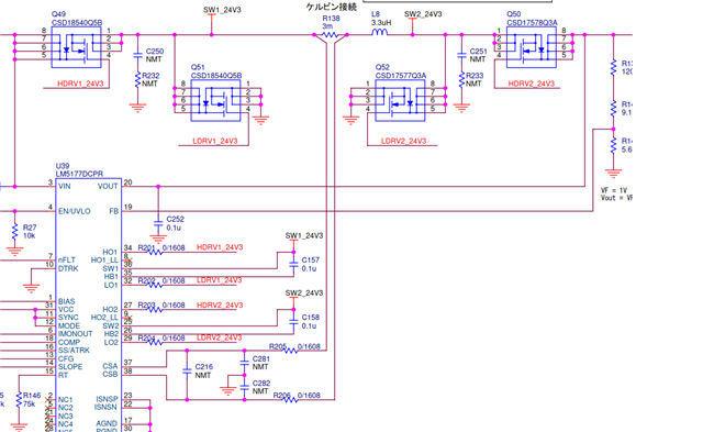
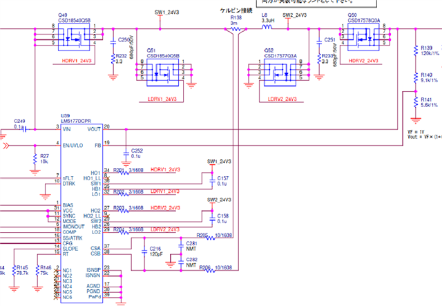
We changed the Nch transistor gate resistor as 0 ohm to 3 ohm.

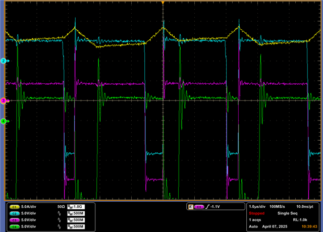
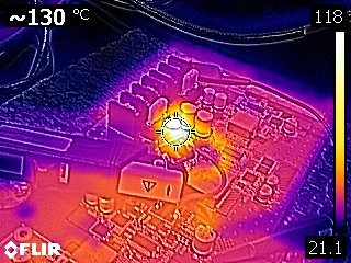
It worked. Before change the value ,anomaly heating inductor less than VIN=20.8V,

after change the value, the phenomena didn't occur even if VIN=26V.

We really appreciate your support.

Best regards,

Satoru Oku

  • HI Satoru,

    sorry, I am not sure if I understood the actual issue right.

    Can you please give some more information what is not working and what you would expect.

    Best regards,

     Stefan

  • Hello, Stefan.

    We discussed in the topic of 

    https://e2e.ti.com/support/power-management-group/power-management/f/power-management-forum/1446780/lm5177-anomaly-heating-phenomena-of-the-inductor-in-dcdc-converter-circuit/5661606#5661606

    We have an issue of anomaly inductor heating.

    When VIN is high (over than 19.5V) , this phenomena happens.

    As you mentioned , this phenomena occurs because of the current loop

    of CSA/CSB line is disturbed.

    So we made the filter of CSA/CSB line using 10 ohm and 120pF.

    Next, the trace of SW node close to CSA/CSB, so cut the line and reconnect using

    wire through the air.(not on PCB)

    After that, you advised snubber construction. so we made it.

    The result was before some change , VIN>19.5V phenome happens, after some change,

    VIN>20.8V phenome happens. So a little improved, but not so enough.

    Finally, we would some additionally change of snubber, but we change the gate drive

    resistor of NMOS.

    Best regards,

    Satoru Oku

    Final schematic and wave form result.

  • HI Satoru,

    so if understood it right, the first two images are before the rework and the second are after the rework.

    So the results are much better and esp. the inductor current would look like expected.

    The ringing you see on the other signals are might be due to the connection of the probe (having a large ground loop).


    So my understanding is that you still see the inductor heating up for higher input voltages (> 20.8V) - right?

    But this is only on  few PCBs - right?

    How much does it heat up?

    Can you share scope plots of SW1 and SW2  and inductor current in the for the setup where you see the inductor heating up. (share a scope plot of a good and a bad unit)  - showing a few switching cycle ~ 5-8.

    Best regards,

     Stefan

  • Hello, Stefan.

    >So my understanding is that you still see the inductor heating up for higher input voltages (> 20.8V) - right?

    Answer is "No".  After change the resistor value of from R201 to R204 as 0 ohm to 3 ohm,

    inductor is not so much heated up when VIN=25 or 26V.

    >But this is only on  few PCBs - right?

    Yes, that's right. 2 of 8 PCBs have this phenomena. And then similar 7 circuits are on same PCB,

    and the only output voltage is different, but only this 24V generate circuit always heat up.

    >How much does it heat up?

    it is over 100 C degree(212 F degree). (before improvement)

    After improvement, it is around 35C degree(95F degree)

    >Can you share scope plots of SW1 and SW2  and inductor current in the for the setup where you see the >inductor heating up. (share a scope plot of a good and a bad unit)  - showing a few switching cycle ~ 5-8.

    How about these pictures. These are picture of same PCB. Before improvement and

    after improvement (we don't have good PCB.)

    Before improvement

    Yellow = inductor current  Sky blue = maybe gate of Q50? Pink = maybe gate of Q52

    After improvement

    Yellow = inductor current  Sky blue = SW1 Pink = SW2 Green = gate of Q50

    Best regards,

    Satoru Oku

  • Hi Satoru,

    really sorry but I still have understanding issues.

    Let me try to describe where:

    1.

    I asked : >So my understanding is that you still see the inductor heating up for higher input voltages (> 20.8V) - right?

    You answered:  Answer is "No". ...

    => So all is OK now - at least this is what I read here

    2.

    I asked : >How much does it heat up?

    You answered:  it is over 100 C degree(212 F degree). (before improvement)

    After improvement, it is around 35C degree(95F degree)

    => So all is OK now - at least this is what I read here

    3.

    You answered:  How about these pictures. These are picture of same PCB. Before improvement and after improvement (we don't have good PCB.)

    => what is meant with " we don't have good PCB."  -   All PCBs are failing now ?

    Best regards,

     Stefan

  • Hello, Stefan.

    It seems our answer made you confuse.

    We made 8 PCBs , and then 6 PCBs are good (no inductor is heating up),

    so we have already delivered to these PCBs our customer.  (another one PCB is broken by our

    analysis failure.)

    We rent only one PCB (inductor is heating up). So we have just one PCB now.

    Best regards,

    Satoru Oku

  • Hi Satoru,

    thanks for the update - better understand now.

    So in this case i would expect one or more of the components on the PCB are damaged and would first try to replace them.

    I suggest to start with replacing the MOSFETs (all of the power stage) and check if this fixes is heating.

    Next the controller LM5177.

    Best regards,

     Stefan