


Other Parts Discussed in Thread: , TIDA-050047
Tool/software:
Hi,
I am developing a portable system which uses a 2S2P battery pack, and I wanted to use BQ25798 for battery charging. After going through the datasheet several times and looking at TIDA-050047 and BQ25798EVM user guide, I think I have more or less arrived at what I need, but I would like to double check before making this, as I saw other forum posts where people managed to turn this IC into BBQ.
The use case is the following: I have a battery powered system that I want to charge from time to time. Whether or not the system stays online during charging is not important to me. I want to be able to charge it only from a single source, USB-C. There is a MCU on the board as well, which I can connect to the I2C of the BQ25798 to configure it, but preferably I would do without it. The datasheet mentions it is capable of doing a full charge cycle without I2C configuration.
Here is the schematic I have:
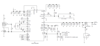
Firstly, the extra pins you may notice, for example, STAT is 1 and 30 has to do with Siemens Mentor pad definitions and the odd shape of landing pad, this is by far the easiest way for me to create them in corners of IC.
Regarding connections:
9.3.5.2 VBUS Input Only section states to connect VAC1,VAC2 to VBUS and ACDRV1,ACDRV2 to GND if there is a single input.
PROG has 6.04k to select 1.5MHz switching and use 1uH inductor
ILIM_HZ by default has the S4 closed, 20k in parallel with 34k giving 12k, and in the end setting max current to 2.1A. When switch is open calculation comes out to 2.75A. This is for flexibility, I am not sure about the thermal situation of the battery yet. I understand these can also change a bit depending on the VBUS, since typical value for REGN is 4.8V with VBUS of 5V, and typical value of 5V with a higher VBUS, but that is taken into account.
S5 is a physical switch to power off the device, so in my mind it made sense to put it and SYS output.
Reading 9.3.3 Device Power Up from Battery without Input Source and 9.3.4 Device Power Up from Input Source, I am not sure if the POR sequence happens when I plug/unplug USB cable?
From 9.3.4.5.1 D+/D– Detection Sets Input Current Limit, if I understand correctly, for non standard adapters I need to create a voltage divider on D+ and D- pins to set the max input current, and for DCP I need to set the EN_9V and EN_12V registers through I2C?
In the use scenario I described, I think SDRV is not of much use to me so I tied it to GND with C65.
Looking at the schematic and the simple use case I described, is there anything else I should consider here, is there something obvious I have missed? Perhaps something else makes more sense?
Best regards,
TI Enthusiast