This thread has been locked.

If you have a related question, please click the "Ask a related question" button in the top right corner. The newly created question will be automatically linked to this question.

TPS25751EVM: TPS25751EVM

Part Number: TPS25751EVM
Other Parts Discussed in Thread: TPS25751

Tool/software:

Hi team:

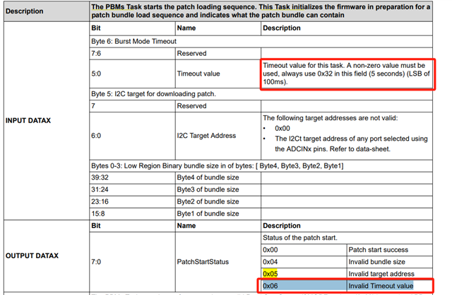
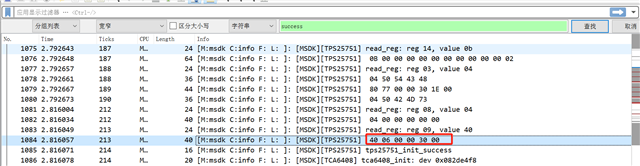
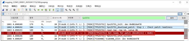
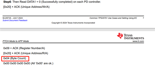
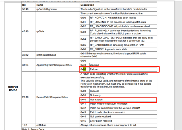
I encountered an error while downloading the patch bundle. When executing step six to read the 0x09 register, it should have returned 0x00 for all, but mine is not. The first number I returned was 0x06. According to the datasheet, 0x06 represents the invalid timeout value, but the timeout value is indicated in the datasheet to be set to 0x32, which makes me confused. I would like to ask what the timeout value should be defined as?

  • Hi,

    We will get back to you next week as TI US is on holiday.

    Regards

  • Hi Tommy Lin,

    Thank you for your update. I appreciate the notice and will await your follow-up next week.
    Please don't hesitate to reach out if you need any additional information from our side in the meantime.
    Best Regards!
    Iris
  • Hi Li, 

    Could you share the values written to Input DataX and the Output DataX read value?

    Best Regards, 

    Aya Khedr

  • Hi Aya Khedr,

    The following is the code for downloading patches and the output data. The image represents the log output after step six。

    Best Regards!

    Iris

    int tps25751_download_patch_bundle(const msdk_device_t *dev, const uint8_t *patch_data, size_t patch_size)
    {
        int ret;
        uint8_t buf[64];
        // Step 1: Check ReadyForPatch bit (INT_EVENT1, Reg 0x14, Byte 11, Bit 1 = 0x02)
        memset(buf, 0, sizeof(buf));
        ret = read_reg(dev, 0x14, buf, 12);
        if (ret != MSDK_STATUS__OK || (buf[11] & 0x02) == 0) {
            MSDK_LOG_ERR("Not ready for patch (0x14h != 0x02)");
            return MSDK_STATUS__ERROR;
        }
        MSDK_LOG_DBG(" %02X %02X %02X %02X %02X %02X %02X %02X %02X %02X %02X %02X", buf[0], buf[1], buf[2], buf[3], buf[4], buf[5],buf[6], buf[7], buf[8], buf[9], buf[10], buf[11]);
    
        // Step 2: Check current mode == 'PTCH'
        memset(buf, 0, sizeof(buf));
        ret = read_reg(dev, 0x03, buf, 5);
        if (ret != MSDK_STATUS__OK || strncmp((char *)&buf[1], "PTCH", 4) != 0) {
            MSDK_LOG_ERR("Not in PTCH mode, got %.4s", &buf[1]);
            return MSDK_STATUS__ERROR;
        }
        MSDK_LOG_DBG(" %02X %02X %02X %02X %02X ", buf[0], buf[1], buf[2], buf[3], buf[4]);
    
        // Step 3: Write DATA1 = [size_LSB...MSB][target][timeout]
        memset(buf, 0, sizeof(buf));
        buf[0] = (uint8_t)(patch_size & 0xFF);
        buf[1] = (uint8_t)((patch_size >> 8) & 0xFF);
        buf[2] = (uint8_t)((patch_size >> 16) & 0xFF);
        buf[3] = (uint8_t)((patch_size >> 24) & 0xFF);
        buf[4] = 0x30;  // Patch I2C target address (must be different from default)
        buf[5] = 0x32;  // Timeout = 5s = 0x32 * 100ms
        ret = write_reg(dev, 0x09, buf, 6);
        if (ret != MSDK_STATUS__OK) return ret;
        msdk_time_delay_ms(10);
        MSDK_LOG_DBG(" %02X %02X %02X %02X %02X %02X %02X", buf[0], buf[1], buf[2], buf[3], buf[4], buf[5], buf[6]);
    
        // Step 4: Write CMD1 = 'PBMs'
        uint8_t pbms_cmd[5] = {0x04, 'P', 'B', 'M', 's'};
        ret = write_reg(dev, 0x08, pbms_cmd, 5);
        if (ret != MSDK_STATUS__OK) return ret;
        MSDK_LOG_DBG(" %02X %02X %02X %02X %02X", pbms_cmd[0], pbms_cmd[1], pbms_cmd[2], pbms_cmd[3], pbms_cmd[4]);
    
        msdk_time_delay_ms(10); // Wait 10ms
    
        // Step 5: Poll CMD1 (0x08) until cleared
        for (int i = 0; i < 10; i++) {
            memset(buf, 0, sizeof(buf));
            ret = read_reg(dev, 0x08, buf, 5);
            if (ret == MSDK_STATUS__OK && buf[1] == 0x00) break;
            msdk_time_delay_ms(5);
        }
        if (buf[1] != 0x00) {
            MSDK_LOG_ERR("PBMs command did not clear CMD1, buf[1]=0x%02X", buf[1]);
            return MSDK_STATUS__ERROR;
        }
    
        msdk_time_delay_ms(5);
        // Step 6: Check if DATA1 status is 0
        memset(buf, 0, sizeof(buf));
        ret = read_reg(dev, 0x09, buf, 5);
        MSDK_LOG_DBG(" %02X %02X %02X %02X %02X %02X", buf[0], buf[1], buf[2], buf[3], buf[4], buf[5]);
        if (ret != MSDK_STATUS__OK || buf[1] != 0x00) return MSDK_STATUS__ERROR;
    
    
        // Step 7: Write Patch Data to I2C addr 0x30 register 0x01 (burst)
        size_t offset = 0;
        const size_t chunk_size = 16;
        while (offset < patch_size) {
            size_t len = (patch_size - offset > chunk_size) ? chunk_size : patch_size - offset;
            ret = msdk_i2c_write_reg(dev, 0x30, 0x01, (uint8_t *)&patch_data[offset], len);
            if (ret != MSDK_STATUS__OK) {
                MSDK_LOG_ERR("Failed writing patch at offset 0x%X", (unsigned)offset);
                return ret;
            }
            offset += len;
        }
    
        msdk_time_delay_ms(10); // Wait 10ms
    
        // Step 8: Write CMD1 = 'PBMc' to complete
        uint8_t pbmc_cmd[5] = {0x04, 'P', 'B', 'M', 'c'};
        ret = write_reg(dev, 0x08, pbmc_cmd, 5);
        if (ret != MSDK_STATUS__OK) return ret;
    
        // Step 9: Confirm CMD1 is cleared
        memset(buf, 0, sizeof(buf));
        ret = read_reg(dev, 0x08, buf, 5);
        if (ret != MSDK_STATUS__OK || buf[1] != 0x00) return MSDK_STATUS__ERROR;
    
        // Step 10: Confirm DATA1 status is 0
        memset(buf, 0, sizeof(buf));
        ret = read_reg(dev, 0x09, buf, 5);
        if (ret != MSDK_STATUS__OK || buf[1] != 0x00) return MSDK_STATUS__ERROR;
    
        // Step 11: Check Mode = 'APP '
        memset(buf, 0, sizeof(buf));
        ret = read_reg(dev, 0x03, buf, 6);
        if (ret != MSDK_STATUS__OK || strncmp((char *)&buf[1], "APP ", 4) != 0) {
            MSDK_LOG_ERR("Patch success but still not in APP mode, got: %.4s", &buf[1]);
            return MSDK_STATUS__ERROR;
        }
    
        MSDK_LOG_INF("TPS25751 patch bundle loaded successfully, device is in APP mode");
        return MSDK_STATUS__OK;
    }

  • Hi Li, 

    Could you share the full I2C log? I can see the register read values but would like to see the writes as well if possible. 

    Best Regards, 

    Aya Khedr

  • Hi Aya Khedr,

    Here are all the logs we output. After opening the document, you can search for "tps25751" to view the logs related to tps25751.

    Best Regards!

    Iris

    tps25751.txt

  • Hi Li,

    Thank you for providing. I will review and get back to you with feedback by end of week.

    Best Regards, 

    Aya Khedr 

  • Hi Aya Khedr,

    That's OK. Thank you very much!

    Best Regards!

    Iris

  • Hi Li,

    No problem. 

    Best Regards, 

    Aya Khedr

  • Hi Aya Khedr,
    Due to the project schedule, we hope to receive your reply as soon as possible. We hope for your understanding and thank you very much!

    Best Regards!

    Iris

  • Hi Aya Khedr,
    Due to the project schedule, we hope to receive your reply as soon as possible. We hope for your understanding and thank you very much!

    Best Regards!

    Iris

  • Hi Aya Khedr,
    Due to the project schedule, we hope to receive your reply as soon as possible. We hope for your understanding and thank you very much!

    Best Regards!

    Iris

  • BTW.. Are you doing this on EVM? EVM has an EEPROM already on it.

  • Hi Li, 

    To add on to Ghouse's question, my assumption is that you have the EEPROM disconnected on the EVM (removing JP16), correct? 

    While reviewing the logs, I noticed that in Step 3, writing to DATAX register seems to be incorrect. 

    859 1.861693 190 MCU 24 [M:msdk C:info F: L: ]: [MSDK][TPS25751] write_reg: reg 09, value 80
    860 1.861695 200 MCU 44 [M:msdk C:info F: L: ]: [MSDK][TPS25751] 80 77 00 00 30 32 00

    The first byte should be the byte count which is 06 and not 80. The timeout value should be in Byte 6. 

    Best Regards, 

    Aya Khedr 

  • Hi Ghouse,
    Yes, we conducted the test on EVM!

    Best Regards!
    Iris

  • Hi Aya Khedr,
    You're right, we disconnected the EEPROM and unplugged the J16 jumper cap。If the EEPROM is not turned on. An error will occur in the first step, as shown in the figure


    Best Regards!
    Iris!

  • Hi Li, 

    Could you clarify when the error occurs? Is this when J16 is connected?

    Best Regards, 

    Aya Khedr 

  • Hi Li,

    We have identified the issue. There was an error when writing to the register in step. buf [0] should have been passed in as 06, but we passed it in incorrectly
    Thank you very much for your support!

    Best Regards!
    Iris

  • Hi Aya Khedr,

    Hello, we encountered an error during the tenth step, which showed that the patch was invalid. The following is the code and log. You can search for tps25751 in the logCould you please help us identify where the problem occurred? Thank you very much!

    Best Regards!

    Iris

    1083	2.750893	1371	MCU	24	[M:msdk C:info F: L: ]: [MSDK][TPS25751] read_reg: reg 14, value 0b
    1084	2.750902	1371	MCU	16	[M:msdk C:info F: L: ]: [MSDK][TPS25751] INT_EVENT1 ReadyForPatch bit is ready for patching.
    1085	2.750906	1371	MCU	64	[M:msdk C:info F: L: ]: [MSDK][TPS25751] Step 1:  0B 00 00 00 00 00 00 00 00 00 00 02
    1086	2.750916	1373	MCU	28	[M:hal C:info F: L: ]: [HAL audio] Send msg 700001 0, wait count 2 \r\n
    1087	2.750921	1373	MCU	24	[M:msdk C:info F: L: ]: [MSDK][TPS25751] read_reg: reg 03, value 04
    1088	2.750925	1373	MCU	16	[M:msdk C:info F: L: ]: [MSDK][TPS25751] PD controller is ready for patching.
    1089	2.750937	1373	MCU	36	[M:msdk C:info F: L: ]: [MSDK][TPS25751] Step 2: 04 50 54 43 48 
    1090	2.750945	1374	DSP	28	[M:dsp_mw C:info F: L: ]: [Audio Dump] CCNI ID: 700001, Dump Mask: 0, SendID: 1
    1091	2.750949	1374	DSP	20	[M:dsp_mw C:info F: L: ]: [Audio Dump] DumpIdCfgVersion = 0
    1092	2.750956	1375	MCU	24	[M:msdk C:info F: L: ]: [MSDK][TPS25751] write_reg: reg 09, value 06
    1093	2.750960	1375	MCU	44	[M:msdk C:info F: L: ]: [MSDK][TPS25751]  Step 3: 06 80 33 00 00 35 32
    1094	2.750967	1375	MCU	28	[M:hal C:info F: L: ]: [HAL audio] Send msg 700002 1, wait count 2 \r\n
    1095	2.750971	1375	MCU	20	[M:AudSrc C:info F: L: ]: [Sink][Setting]init--ver: 0
    1096	2.750975	1375	MCU	20	[M:AudSrc C:info F: L: ]: [Sink][Setting]eaps_reg--cid: 0x0423f98c
    1097	2.750979	1376	DSP	28	[M:dsp_mw C:info F: L: ]: [Audio Dump] CCNI ID: 700002, Dump Mask: 1, SendID: 2
    1098	2.750983	1376	DSP	20	[M:dsp_mw C:info F: L: ]: [Audio Dump] AudioDumpDevice = 1
    1099	2.750986	1376	MCU	24	[M:AudSrc C:info F: L: ]: [Sink][Setting]audio_get_max_sound_level_out volType:0 totalLevel:16\n
    1100	2.750991	1377	MCU	24	[M:AudSrc C:info F: L: ]: [Sink][Setting]audio_get_max_sound_level_out volType:5 totalLevel:16\n
    1101	2.750995	1378	MCU	24	[M:AudSrc C:info F: L: ]: [Sink][Setting]audio_get_max_sound_level_out volType:7 totalLevel:16\n
    1102	2.750998	1379	MCU	24	[M:AudSrc C:info F: L: ]: [Sink][Setting]audio_get_max_sound_level_out volType:8 totalLevel:16\n
    1103	2.751002	1381	MCU	24	[M:AudSrc C:info F: L: ]: [Sink][Setting]audio_get_max_sound_level_in volType:11 totalLevel:16\n
    1104	2.751006	1382	MCU	24	[M:AudSrc C:info F: L: ]: [Sink][Setting]audio_get_max_sound_level_out volType:10 totalLevel:16\n
    1105	2.751010	1383	MCU	28	[M:hal C:info F: L: ]: [HAL audio] Send msg 260000 24224898, wait count 1 \r\n
    1106	2.751014	1383	MCU	24	[M:hal C:info F: L: ]: [HAL audio] Wait msg(0x26) ack 0 \r\n
    1107	2.751018	1383	MCU	24	[M:msdk C:info F: L: ]: [MSDK][TPS25751] write_reg: reg 08, value 04
    1108	2.751022	1383	MCU	36	[M:msdk C:info F: L: ]: [MSDK][TPS25751] Step 4: 04 50 42 4D 73
    1109	2.751028	1383	DSP	32	[M:hal C:info F: L: ]: Audio Gain Offset Gain0:0, Gain1:0, Gain2:0, Gain3:0, \r\n
    1110	2.751034	1383	DSP	32	[M:hal C:info F: L: ]: Audio Gain Offset Gain4:0, Gain5:0, Gain6:0, Gain7:0, \r\n
    1111	2.751038	1383	MCU	28	[M:hal C:info F: L: ]: [HAL audio] Receive msg 8026, 0, 0 \r\n
    1112	2.751042	1384	MCU	24	[M:hal C:info F: L: ]: [HAL audio] Ack 26, wait count 1 \r\n
    1113	2.751046	1384	MCU	20	[M:AudSrc C:info F: L: ]: [Sink][AM]audio_set_param_hdlr with feature type 0x80\n
    1114	2.751050	1384	MCU	28	[M:hal C:info F: L: ]: [HAL audio] Send msg 4b0000 0, wait count 1 \r\n
    1115	2.751057	1385	MCU	20	[M:AudSrc C:info F: L: ]: [Sink][AM]audio_set_param_hdlr with feature type 0x1\n
    1116	2.751060	1385	MCU	16	[M:AudSrc C:info F: L: ]: [Sink][AM] Init: DC Compensation\n
    1117	2.751063	1385	MCU	20	[M:hal C:info F: L: ]: [stream out] Audio_or_Voice = 0
    1118	2.751066	1385	MCU	20	[M:hal C:info F: L: ]: [stream out] audio_device = 768
    1119	2.751068	1385	MCU	20	[M:hal C:info F: L: ]: [stream out] audio_interface = 0
    1120	2.751082	1385	MCU	20	[M:hal C:info F: L: ]: [stream out] stream_channel = 0
    1121	2.751086	1385	MCU	20	[M:hal C:info F: L: ]: [stream out] bias0_1_2_with_LDO0 = 0
    1122	2.751088	1385	MCU	16	[M:AudSrc C:info F: L: ]: [AMI] ami_hal_mutex_lock() +\r\n
    1123	2.751113	1385	MCU	28	[M:hal C:info F: L: ]: [Audio Clock] scenario type = [23] param = 0x4224880 enable = [1] 
    1124	2.751119	1385	MCU	79	[M:hal C:info F: L:]
    : [PMU_AUDIO]VAUD18 vol before[900][1300][1800]
    1125	2.751130	1385	MCU	78	[M:hal C:info F: L:]
    : [PMU_AUDIO]VAUD18 vol after[900][1300][1800]
    1126	2.751139	1386	MCU	24	[M:hal C:info F: L: ]: [PMU_AUDIO]vsel[0], volt[900]
    1127	2.751143	1386	MCU	24	[M:hal C:info F: L: ]: [PMU_AUDIO]vsel[2], volt[1800]
    1128	2.751145	1386	MCU	16	[M:hal C:info F: L: ]: [PMU_AUDIO]set_audio_mode, CLASS G2
    1129	2.751147	1386	MCU	20	[M:hal C:info F: L: ]: [PMU_AUDIO]set_audio_mode, AUDIO_MODE[0x1]
    1130	2.751150	1387	MCU	24	[M:hal C:info F: L: ]: [PMU_AUDIO]set_audio_mode, VSEL_L[0x19], IPEAK_L[0x1]
    1131	2.751153	1387	MCU	24	[M:hal C:info F: L: ]: [PMU_AUDIO]set_audio_mode, VSEL_M[0x41], IPEAK_M[0x1]
    1132	2.751155	1387	MCU	24	[M:hal C:info F: L: ]: [PMU_AUDIO]set_audio_mode, VSEL_H[0x73], IPEAK_H[0x4]
    1133	2.751161	1388	MCU	20	[M:hal C:info F: L: ]: [PMU_PWR]switch_power, After VAUD18 status[0x0A]
    1134	2.751164	1390	MCU	20	[M:hal C:info F: L: ]: [PMU_PWR]switch_power, After VAUD18 status[0x0C]
    1135	2.751166	1390	MCU	20	[M:hal C:info F: L: ]: [Audio Clock] enable dac type 23
    1136	2.751169	1390	MCU	24	[M:hal C:info F: L: ]: [Audio Clock] low jitter mode: i2s in device is not suitable, type 23 device 0x0
    1137	2.751172	1390	MCU	24	[M:hal C:info F: L: ]: [Audio Clock] low jitter mode: i2s_out device is not suitable, type 23 device 0x300
    1138	2.751174	1390	MCU	16	[M:hal C:info F: L: ]: [Audio Clock] lock SPM state1
    1139	2.751177	1390	MCU	32	[M:hal C:info F: L: ]: [SLP] spm_force_sleep_state: caller=0, sleep state=0, sleep control=1, lock sleep state status=0x00000001
    1140	2.751182	1390	MCU	24	[M:hal C:info F: L: ]: [SLP] spm_control_mtcmos=2, control=1\r\n
    1141	2.751184	1390	MCU	24	[M:hal C:info F: L: ]: [SLP] spm_control_mtcmos=3, control=1\r\n
    1142	2.751186	1390	MCU	24	[M:hal C:info F: L: ]: [SLP] spm_control_mtcmos=4, control=1\r\n
    1143	2.751188	1390	MCU	20	[M:hal C:info F: L: ]: [Audio Clock][AMP] lock clock [24]!
    1144	2.751194	1391	MCU	16	[M:hal C:info F: L: ]: [Audio Clock] lock SPM state4
    1145	2.751199	1391	MCU	32	[M:hal C:info F: L: ]: [SLP] spm_force_sleep_state: caller=0, sleep state=2, sleep control=1, lock sleep state status=0x01000001
    1146	2.751202	1391	MCU	16	[M:hal C:info F: L: ]: [Audio Clock][AMP] lock common audio clock
    1147	2.751205	1391	MCU	28	[M:hal C:info F: L: ]: [Audio Clock] type [23] cg_setting [0x5000007] control [0x1]
    1148	2.751210	1391	MCU	80	[M:hal C:info F: L: ]: [Audio Clock] DAC [0x0][0x0][0x0][0x800002] INT [0x0][0x0][0x0][0x800002] ENGINE [0x0][0x0][0x0][0x800002] GPSRC [0x0][0x0][0x0][0x800002]
    1149	2.811938	1391	MCU	80	[M:hal C:info F: L: ]: [Audio Clock] UL  [0x0][0x0][0x0][0x0] DL  [0x0][0x0][0x0][0x0] SPDIF  [0x0][0x0][0x0][0x0] TEST  [0x0][0x0][0x0][0x0]
    1150	2.811949	1391	MCU	80	[M:hal C:info F: L: ]: [Audio Clock] APLL2 IN [0x0][0x0][0x0][0x0] APLL1 IN [0x0][0x0][0x0][0x0] APLL2 OUT [0x0][0x0][0x0][0x0] APLL1 OUT [0x0][0x0][0x0][0x0]
    1151	2.811954	1391	MCU	80	[M:hal C:info F: L: ]: [Audio Clock] Bias0_HP [0x0][0x0][0x0][0x0] Bias1_HP [0x0][0x0][0x0][0x0] Bias2_HP [0x0][0x0][0x0][0x0] Bias0_NM [0x0][0x0][0x0][0x0]
    1152	2.811957	1391	MCU	80	[M:hal C:info F: L: ]: [Audio Clock] Bias1_NM [0x0][0x0][0x0][0x0] Bias2_NM [0x0][0x0][0x0][0x0] Bias0_LP [0x0][0x0][0x0][0x0] Bias1_LP [0x0][0x0][0x0][0x0]
    1153	2.811960	1391	MCU	48	[M:hal C:info F: L: ]: [Audio Clock] Bias2_LP [0x0][0x0][0x0][0x0] VOW [0x0][0x0][0x0][0x0]
    1154	2.811963	1391	MCU	80	[M:hal C:info F: L: ]: [Audio Clock] SPM State1 [0x0][0x0][0x0][0x800000] State3 [0x0][0x0][0x0][0x0] State4 [0x0][0x0][0x0][0x2]
    1155	2.811967	1391	MCU	16	[M:AudSrc C:info F: L: ]: [AMI] ami_hal_mutex_lock() -\r\n
    1156	2.811970	1391	MCU	28	[M:hal C:info F: L: ]: [HAL audio] Send msg 20480000 24261ef4, wait count 1 \r\n
    1157	2.812016	1391	MCU	24	[M:hal C:info F: L: ]: [HAL audio] Wait msg(0x2048) ack 0 \r\n
    1158	2.812020	1391	MCU	24	[M:msdk C:info F: L: ]: [MSDK][TPS25751] read_reg: reg 08, value 04
    1159	2.812026	1391	MCU	40	[M:msdk C:info F: L: ]: [MSDK][TPS25751] Step 5: 04 00 00 00 00 00
    1160	2.812030	1392	DSP	16	[M:dsp_mw C:info F: L: ]: [DC COMPENSATION] Start\r\n
    1161	2.812033	1392	DSP	24	[M:hal C:info F: L: ]: DSP - Hal Audio Output Mode Setting, gain_select:0x0, dac_mode:0x0
    1162	2.812036	1392	DSP	24	[M:hal C:info F: L: ]: DSP - Hal Audio Volume Select:0, mode:0
    1163	2.812038	1392	DSP	28	[M:hal C:info F: L: ]: hal_device_convert_agent 768 if 0 is_tx 0
    1164	2.812040	1392	DSP	24	[M:hal C:info F: L: ]: hal_device_convert_device_agent 768 if 0
    1165	2.812042	1392	DSP	36	[M:hal C:info F: L: ]: #hal_audio_device_set_agent# device 0x300, agent 58, device_agent 7, type 0, on/off 1
    1166	2.812044	1392	DSP	24	[M:dsp_mw C:info F: L: ]: [DSP AMP] afe_send_amp_status_ccni [0x22410001], ack success from isr 0\r\n
    1167	2.812048	1392	DSP	20	[M:hal C:info F: L: ]: [Audio Agent] DSP - Hal Audio AFE control:1
    1168	2.812050	1392	DSP	24	[M:hal C:info F: L: ]: afe_set on agnet 58 device 768\r\n
    1169	2.812052	1392	DSP	44	[M:hal C:info F: L: ]: DSP - Hal Audio ANA DAC:0x7, Mode:0, Performance:0, rate:48000, dc_compensation:0x0, first_boot=1, CLASS-G Enable:1
    1170	2.812055	1393	DSP	24	[M:hal C:info F: L: ]: DSP - Hal Audio Volume Select:0, mode:0
    1171	2.812056	1393	DSP	24	[M:hal C:info F: L: ]: [Audio Driver]AFE COMMON GLOBAL, analog_select:0, enable:1
    1172	2.812057	1393	DSP	16	[M:hal C:info F: L: ]: [Audio Driver]AFE COMMON GLOBAL ANALOG INITIAL ON
    1173	2.812059	1393	DSP	20	[M:hal C:info F: L: ]: [Audio Driver]AFE COMMON GLOBAL ANALOG INITIAL STATUS = 0x01
    1174	2.812060	1393	MCU	24	[M:msdk C:info F: L: ]: [MSDK][TPS25751] read_reg: reg 09, value 40
    1175	2.812061	1393	MCU	88	[M:msdk C:info F: L: ]: [MSDK][TPS25751] Step 6: 40 00 00 00 00 00 00 00 00 00 00 00 00 00 00 00 00 00
    1176	2.812065	1393	MCU	20	[M:msdk C:info F: L: ]: [MSDK][TPS25751] tps25751_write_patch patch size 13184
    1177	2.812070	1411	DSP	24	[M:hal C:info F: L: ]: [DEBUG] gain value:0x38e, mapping_value:0x208
    1178	2.812072	1411	DSP	24	[M:hal C:info F: L: ]: DSP - Hal Audio Gain Output Analog Ramp, current:0xaeb, target:0x208
    1179	2.812076	1411	DSP	20	[M:hal C:info F: L: ]: DSP - Hal Audio Gain Output Analog, Gain:0xaaa
    1180	2.812077	1411	DSP	20	[M:hal C:info F: L: ]: DSP - Hal Audio Gain Output Analog, Gain:0xa69
    1181	2.812078	1411	DSP	20	[M:hal C:info F: L: ]: DSP - Hal Audio Gain Output Analog, Gain:0xa28
    1182	2.812079	1411	DSP	20	[M:hal C:info F: L: ]: DSP - Hal Audio Gain Output Analog, Gain:0x9e7
    1183	2.812080	1411	DSP	20	[M:hal C:info F: L: ]: DSP - Hal Audio Gain Output Analog, Gain:0x9a6
    1184	2.812083	1412	DSP	20	[M:hal C:info F: L: ]: DSP - Hal Audio Gain Output Analog, Gain:0x965
    1185	2.812084	1412	DSP	20	[M:hal C:info F: L: ]: DSP - Hal Audio Gain Output Analog, Gain:0x924
    1186	2.812085	1412	DSP	20	[M:hal C:info F: L: ]: DSP - Hal Audio Gain Output Analog, Gain:0x8e3
    1187	2.812088	1412	DSP	20	[M:hal C:info F: L: ]: DSP - Hal Audio Gain Output Analog, Gain:0x8a2
    1188	2.812089	1412	DSP	20	[M:hal C:info F: L: ]: DSP - Hal Audio Gain Output Analog, Gain:0x861
    1189	2.812090	1412	DSP	20	[M:hal C:info F: L: ]: DSP - Hal Audio Gain Output Analog, Gain:0x820
    1190	2.812091	1413	DSP	20	[M:hal C:info F: L: ]: DSP - Hal Audio Gain Output Analog, Gain:0x7df
    1191	2.812092	1413	DSP	20	[M:hal C:info F: L: ]: DSP - Hal Audio Gain Output Analog, Gain:0x79e
    1192	2.812093	1413	DSP	20	[M:hal C:info F: L: ]: DSP - Hal Audio Gain Output Analog, Gain:0x75d
    1193	2.812094	1413	DSP	20	[M:hal C:info F: L: ]: DSP - Hal Audio Gain Output Analog, Gain:0x71c
    1194	2.812096	1413	DSP	20	[M:hal C:info F: L: ]: DSP - Hal Audio Gain Output Analog, Gain:0x6db
    1195	2.812096	1414	DSP	20	[M:hal C:info F: L: ]: DSP - Hal Audio Gain Output Analog, Gain:0x69a
    1196	2.812097	1414	DSP	20	[M:hal C:info F: L: ]: DSP - Hal Audio Gain Output Analog, Gain:0x659
    1197	2.812098	1414	DSP	20	[M:hal C:info F: L: ]: DSP - Hal Audio Gain Output Analog, Gain:0x618
    1198	2.812099	1414	DSP	20	[M:hal C:info F: L: ]: DSP - Hal Audio Gain Output Analog, Gain:0x5d7
    1199	2.812100	1414	DSP	20	[M:hal C:info F: L: ]: DSP - Hal Audio Gain Output Analog, Gain:0x596
    1200	2.812101	1414	DSP	20	[M:hal C:info F: L: ]: DSP - Hal Audio Gain Output Analog, Gain:0x555
    1201	2.812102	1415	MCU	28	[M:hal C:info F: L: ]: [HAL audio] Receive msg 2241, 1, 0 \r\n
    1202	2.812104	1415	MCU	24	[M:AudSrc C:info F: L: ]: [AudM]msg_id = 17, fromISR = 1
    1203	2.812105	1415	DSP	20	[M:hal C:info F: L: ]: DSP - Hal Audio Gain Output Analog, Gain:0x514
    1204	2.812106	1415	DSP	20	[M:hal C:info F: L: ]: DSP - Hal Audio Gain Output Analog, Gain:0x4d3
    1205	2.812107	1415	DSP	20	[M:hal C:info F: L: ]: DSP - Hal Audio Gain Output Analog, Gain:0x492
    1206	2.812108	1415	DSP	20	[M:hal C:info F: L: ]: DSP - Hal Audio Gain Output Analog, Gain:0x451
    1207	2.812109	1415	DSP	20	[M:hal C:info F: L: ]: DSP - Hal Audio Gain Output Analog, Gain:0x410
    1208	2.812109	1416	DSP	20	[M:hal C:info F: L: ]: DSP - Hal Audio Gain Output Analog, Gain:0x3cf
    1209	2.812125	1416	DSP	20	[M:hal C:info F: L: ]: DSP - Hal Audio Gain Output Analog, Gain:0x38e
    1210	2.812127	1416	DSP	20	[M:hal C:info F: L: ]: DSP - Hal Audio Gain Output Analog, Gain:0x34d
    1211	2.812129	1416	DSP	20	[M:hal C:info F: L: ]: DSP - Hal Audio Gain Output Analog, Gain:0x30c
    1212	2.812130	1416	DSP	20	[M:hal C:info F: L: ]: DSP - Hal Audio Gain Output Analog, Gain:0x2cb
    1213	2.812131	1416	DSP	20	[M:hal C:info F: L: ]: DSP - Hal Audio Gain Output Analog, Gain:0x28a
    1214	2.812132	1417	DSP	20	[M:hal C:info F: L: ]: DSP - Hal Audio Gain Output Analog, Gain:0x249
    1215	2.812133	1417	DSP	20	[M:hal C:info F: L: ]: DSP - Hal Audio Gain Output Analog, Gain:0x208
    1216	2.812134	1422	DSP	16	[M:hal C:info F: L: ]: CLASS-G ON FINISH
    1217	2.812135	1422	DSP	28	[M:hal C:info F: L: ]: analog_out_select=0,L=1,R=1
    1218	2.812138	1422	DSP	20	[M:hal C:info F: L: ]: [Audio Agent] DSP - HAL_AUDIO_AFE_CLOCK_DAC:1
    1219	2.812139	1422	DSP	20	[M:hal C:info F: L: ]: [Audio Agent] DSP - HAL_AUDIO_AFE_CONTROL_ADDA:1
    1220	2.812140	1422	DSP	24	[M:hal C:info F: L: ]: [DEBUG] gain value:0x38e, mapping_value:0x208
    1221	2.812142	1422	DSP	20	[M:hal C:info F: L: ]: DSP - Hal Audio Gain Output Analog, Gain:0x208
    1222	2.812142	1422	DSP	16	[M:hal C:info F: L: ]: [NLE GAIN OFF] apply nle gain off \r\n
    1223	2.812149	1422	DSP	16	[M:hal C:info F: L: ]: [NLE ON] turn on nle\r\n
    1224	2.812150	1423	DSP	24	[M:hal C:info F: L: ]: DSP - Hal Audio device:0x300, Off/On:1
    1225	2.812152	1423	DSP	24	[M:dsp_mw C:info F: L: ]: AUDDEC_ANA_CON11 addr:0x4209012c val:0x18e\r\n
    1226	2.812154	1423	DSP	28	[M:dsp_aud_msg C:warning F: L: ]: [RX_AUD_MSG] queue_id 1, long callback time:31247 us from rx msg:0x2048
    1227	2.812156	1423	MCU	28	[M:hal C:info F: L: ]: [HAL audio] Receive msg a048, 0, 0 \r\n
    1228	2.812157	1423	MCU	24	[M:hal C:info F: L: ]: [HAL audio] Ack 2048, wait count 16 \r\n
    1229	2.812158	1431	MCU	20	[M:hal C:info F: L: ]: [stream out] Audio_or_Voice = 0
    1230	2.812161	1431	MCU	20	[M:hal C:info F: L: ]: [stream out] audio_device = 768
    1231	2.812162	1431	MCU	20	[M:hal C:info F: L: ]: [stream out] audio_interface = 0
    1232	2.812163	1431	MCU	20	[M:hal C:info F: L: ]: [stream out] stream_channel = 0
    1233	2.812164	1431	MCU	20	[M:hal C:info F: L: ]: [stream out] bias0_1_2_with_LDO0 = 0
    1234	2.812165	1431	MCU	28	[M:hal C:info F: L: ]: [HAL audio] Send msg 204940d0 24261ef4, wait count 1 \r\n
    1235	2.812167	1431	MCU	24	[M:hal C:info F: L: ]: [HAL audio] Wait msg(0x2049) ack 0 \r\n
    1236	2.812168	1431	DSP	16	[M:dsp_mw C:info F: L: ]: [DC COMPENSATION] Stop\r\n
    1237	2.812169	1431	DSP	28	[M:hal C:info F: L: ]: hal_device_convert_agent 768 if 0 is_tx 0
    1238	2.812170	1431	DSP	24	[M:hal C:info F: L: ]: hal_device_convert_device_agent 768 if 0
    1239	2.812171	1431	DSP	36	[M:hal C:info F: L: ]: #hal_audio_device_set_agent# device 0x300, agent 58, device_agent 7, type 0, on/off 0
    1240	2.812173	1432	DSP	24	[M:dsp_mw C:info F: L: ]: [DSP AMP] afe_send_amp_status_ccni [0x22410000], ack success from isr 0\r\n
    1241	2.812181	1432	DSP	16	[M:hal C:info F: L: ]: [NLE GAIN OFF] apply nle gain off \r\n
    1242	2.812183	1432	DSP	16	[M:hal C:info F: L: ]: [NLE OFF] turn off nle\r\n
    1243	2.812185	1432	DSP	44	[M:hal C:info F: L: ]: DSP - Hal Audio ANA DAC:0x7, Mode:0, Performance:0, rate:48000, dc_compensation:0x40d0, first_boot=0, CLASS-G Enable:0
    1244	2.812188	1437	DSP	24	[M:hal C:info F: L: ]: DSP - Hal Audio Gain Output Analog Ramp, current:0x208, target:0xb2c
    1245	2.842873	1455	MCU	28	[M:hal C:info F: L: ]: [HAL audio] Receive msg 2241, 0, 0 \r\n
    1246	2.842884	1455	MCU	24	[M:AudSrc C:info F: L: ]: [AudM]msg_id = 17, fromISR = 1
    1247	2.842894	1460	DSP	24	[M:hal C:info F: L: ]: [Audio Driver]AFE COMMON GLOBAL, analog_select:0, enable:0
    1248	2.842899	1460	DSP	20	[M:hal C:info F: L: ]: [Audio Driver]AFE COMMON GLOBAL ANALOG INITIAL STATUS = 0x00
    1249	2.842902	1460	DSP	16	[M:hal C:info F: L: ]: [Audio Driver]AFE COMMON GLOBAL ANALOG INITIAL OFF
    1250	2.842961	1460	DSP	16	[M:hal C:info F: L: ]: CLASS-G OFF FINISH
    1251	2.842987	1460	DSP	28	[M:hal C:info F: L: ]: analog_out_select=0,L=0,R=0
    1252	2.842993	1460	DSP	20	[M:hal C:info F: L: ]: [Audio Agent] DSP - HAL_AUDIO_AFE_CONTROL_ADDA:0
    1253	2.842996	1460	DSP	20	[M:hal C:info F: L: ]: [Audio Agent] DSP - HAL_AUDIO_AFE_CLOCK_DAC:0
    1254	2.843009	1460	DSP	24	[M:hal C:info F: L: ]: DSP - Hal Audio device:0x300, Off/On:0
    1255	2.843014	1460	DSP	24	[M:hal C:info F: L: ]: afe_set off agnet 58 device 768\r\n
    1256	2.843017	1460	DSP	20	[M:hal C:info F: L: ]: [Audio Agent] DSP - Hal Audio AFE control:0
    1257	2.843029	1461	DSP	24	[M:dsp_mw C:info F: L: ]: DC COMPENSATION val:0x40d0, no_delay_flag = 0x0\r\n
    1258	2.843063	1461	DSP	20	[M:hal C:info F: L: ]: DSP - Hal Audio set_amp_delay_timer:2000
    1259	2.843066	1461	DSP	28	[M:dsp_aud_msg C:warning F: L: ]: [RX_AUD_MSG] queue_id 1, long callback time:29728 us from rx msg:0x2049
    1260	2.843071	1461	MCU	28	[M:hal C:info F: L: ]: [HAL audio] Receive msg a049, 0, 0 \r\n
    1261	2.843075	1462	MCU	24	[M:hal C:info F: L: ]: [HAL audio] Ack 2049, wait count 15 \r\n
    1262	2.843078	1462	MCU	16	[M:AudSrc C:info F: L: ]: [AMI] ami_hal_mutex_lock() +\r\n
    1263	2.843082	1462	MCU	28	[M:hal C:info F: L: ]: [Audio Clock] scenario type = [23] param = 0x0 enable = [0] 
    1264	2.843087	1462	MCU	20	[M:hal C:info F: L: ]: [Audio Clock] AMP delay off start time 1461818
    1265	2.843089	1462	MCU	20	[M:hal C:info F: L: ]: [Audio Clock] disable dac type 23
    1266	2.843092	1462	MCU	16	[M:hal C:info F: L: ]: [Audio Clock] unlock SPM state1
    1267	2.843094	1462	MCU	32	[M:hal C:info F: L: ]: [SLP] spm_force_sleep_state: caller=0, sleep state=0, sleep control=0, lock sleep state status=0x01000000
    1268	2.843101	1462	MCU	28	[M:hal C:info F: L: ]: [Audio Clock] type [23] cg_setting [0x0] control [0x0]
    1269	2.843104	1462	MCU	80	[M:hal C:info F: L: ]: [Audio Clock] DAC [0x0][0x0][0x0][0x2] INT [0x0][0x0][0x0][0x2] ENGINE [0x0][0x0][0x0][0x2] GPSRC [0x0][0x0][0x0][0x2]
    1270	2.843131	1462	MCU	80	[M:hal C:info F: L: ]: [Audio Clock] UL  [0x0][0x0][0x0][0x0] DL  [0x0][0x0][0x0][0x0] SPDIF  [0x0][0x0][0x0][0x0] TEST  [0x0][0x0][0x0][0x0]
    1271	2.843206	1462	MCU	80	[M:hal C:info F: L: ]: [Audio Clock] APLL2 IN [0x0][0x0][0x0][0x0] APLL1 IN [0x0][0x0][0x0][0x0] APLL2 OUT [0x0][0x0][0x0][0x0] APLL1 OUT [0x0][0x0][0x0][0x0]
    1272	2.843243	1462	MCU	80	[M:hal C:info F: L: ]: [Audio Clock] Bias0_HP [0x0][0x0][0x0][0x0] Bias1_HP [0x0][0x0][0x0][0x0] Bias2_HP [0x0][0x0][0x0][0x0] Bias0_NM [0x0][0x0][0x0][0x0]
    1273	2.843250	1462	MCU	80	[M:hal C:info F: L: ]: [Audio Clock] Bias1_NM [0x0][0x0][0x0][0x0] Bias2_NM [0x0][0x0][0x0][0x0] Bias0_LP [0x0][0x0][0x0][0x0] Bias1_LP [0x0][0x0][0x0][0x0]
    1274	2.843261	1462	MCU	48	[M:hal C:info F: L: ]: [Audio Clock] Bias2_LP [0x0][0x0][0x0][0x0] VOW [0x0][0x0][0x0][0x0]
    1275	2.843277	1462	MCU	80	[M:hal C:info F: L: ]: [Audio Clock] SPM State1 [0x0][0x0][0x0][0x0] State3 [0x0][0x0][0x0][0x0] State4 [0x0][0x0][0x0][0x2]
    1276	2.843283	1462	MCU	16	[M:AudSrc C:info F: L: ]: [AMI] ami_hal_mutex_lock() -\r\n
    1277	2.843285	1463	MCU	20	[M:AudSrc C:info F: L: ]: [Sink][AM] Init Finish: DC Compensation, cal value 0x40d0\n
    1278	2.843289	1463	MCU	20	[M:AudSrc C:info F: L: ]: [Audio Clock] dsp amp mcu callback, event [2]
    1279	2.843293	1463	MCU	20	[M:AudSrc C:info F: L: ]: [Audio Clock] dsp amp mcu callback, event [0]
    1280	2.843295	1463	MCU	16	[M:AudSrc C:info F: L: ]: [AMI] ami_hal_mutex_lock() +\r\n
    1281	2.843312	1463	MCU	28	[M:hal C:info F: L: ]: [Audio Clock] scenario type = [1] param = 0x0 enable = [0] 
    1282	2.843317	1463	MCU	20	[M:hal C:info F: L: ]: [Audio Clock] AMP delay off stop time 1462921
    1283	2.843320	1463	MCU	20	[M:hal C:info F: L: ]: [Audio Clock] disable dac type 1
    1284	2.843322	1464	MCU	20	[M:hal C:info F: L: ]: [PMU_PWR]switch_power, After VAUD18 status[0x09]
    1285	2.843326	1466	MCU	20	[M:hal C:info F: L: ]: [PMU_PWR]switch_power, After VAUD18 status[0x09]
    1286	2.843328	1466	MCU	24	[M:hal C:info F: L: ]: [SLP] spm_control_mtcmos=2, control=0\r\n
    1287	2.843330	1466	MCU	24	[M:hal C:info F: L: ]: [SLP] spm_control_mtcmos=3, control=0\r\n
    1288	2.843332	1466	MCU	24	[M:hal C:info F: L: ]: [SLP] spm_control_mtcmos=4, control=0\r\n
    1289	2.843334	1466	MCU	16	[M:hal C:info F: L: ]: [Audio Clock] unlock SPM state4
    1290	2.843336	1466	MCU	32	[M:hal C:info F: L: ]: [SLP] spm_force_sleep_state: caller=0, sleep state=2, sleep control=0, lock sleep state status=0x00000000
    1291	2.843339	1466	MCU	28	[M:hal C:info F: L: ]: [Audio Clock] type [1] cg_setting [0x0] control [0x0]
    1292	2.843341	1466	MCU	80	[M:hal C:info F: L: ]: [Audio Clock] DAC [0x0][0x0][0x0][0x0] INT [0x0][0x0][0x0][0x0] ENGINE [0x0][0x0][0x0][0x0] GPSRC [0x0][0x0][0x0][0x0]
    1293	2.843345	1466	MCU	80	[M:hal C:info F: L: ]: [Audio Clock] UL  [0x0][0x0][0x0][0x0] DL  [0x0][0x0][0x0][0x0] SPDIF  [0x0][0x0][0x0][0x0] TEST  [0x0][0x0][0x0][0x0]
    1294	2.843349	1466	MCU	80	[M:hal C:info F: L: ]: [Audio Clock] APLL2 IN [0x0][0x0][0x0][0x0] APLL1 IN [0x0][0x0][0x0][0x0] APLL2 OUT [0x0][0x0][0x0][0x0] APLL1 OUT [0x0][0x0][0x0][0x0]
    1295	2.843353	1467	MCU	80	[M:hal C:info F: L: ]: [Audio Clock] Bias0_HP [0x0][0x0][0x0][0x0] Bias1_HP [0x0][0x0][0x0][0x0] Bias2_HP [0x0][0x0][0x0][0x0] Bias0_NM [0x0][0x0][0x0][0x0]
    1296	2.843358	1467	MCU	80	[M:hal C:info F: L: ]: [Audio Clock] Bias1_NM [0x0][0x0][0x0][0x0] Bias2_NM [0x0][0x0][0x0][0x0] Bias0_LP [0x0][0x0][0x0][0x0] Bias1_LP [0x0][0x0][0x0][0x0]
    1297	2.843361	1467	MCU	48	[M:hal C:info F: L: ]: [Audio Clock] Bias2_LP [0x0][0x0][0x0][0x0] VOW [0x0][0x0][0x0][0x0]
    1298	2.843364	1467	MCU	80	[M:hal C:info F: L: ]: [Audio Clock] SPM State1 [0x0][0x0][0x0][0x0] State3 [0x0][0x0][0x0][0x0] State4 [0x0][0x0][0x0][0x0]
    1299	2.843369	1467	MCU	16	[M:AudSrc C:info F: L: ]: [AMI] ami_hal_mutex_lock() -\r\n
    1300	4.155279	2748	MCU	24	[M:msdk C:info F: L: ]: [MSDK][TPS25751] tps25751_write_patch left patch size 60  00
    1301	4.155296	2755	MCU	16	[M:msdk C:info F: L: ]: [MSDK][LP5864] lp5864_set_bt_led(mode1) success
    1302	4.155301	2756	MCU	24	[M:msdk C:info F: L: ]: [MSDK][TPS25751] write_reg: reg 08, value 04
    1303	4.155307	2756	MCU	40	[M:msdk C:info F: L: ]: [MSDK][TPS25751] Step 8: 04 50 42 4D 63 C7
    1304	4.155370	2757	MCU	24	[M:msdk C:info F: L: ]: [MSDK][TPS25751] read_reg: reg 08, value 04
    1305	4.155394	2758	MCU	16	[M:msdk C:info F: L: ]: [MSDK][TPS25751] Confirm CMD1 is cleared.
    1306	4.155399	2758	MCU	40	[M:msdk C:info F: L: ]: [MSDK][TPS25751]  Step 9 :04 00 00 00 00 00
    1307	4.155405	2758	MCU	16	[M:msdk C:info F: L: ]: [MSDK][LP5864] lp5864_set_m_led(mode1) success
    1308	4.155408	2760	MCU	16	[M:msdk C:info F: L: ]: [MSDK][LP5864] lp5864_set_volume_led(mode1) success
    1309	4.155411	2762	MCU	16	[M:msdk C:info F: L: ]: [MSDK][LP5864] lp5864_set_bass_led(mode1) success
    1310	4.155413	2764	MCU	16	[M:msdk C:info F: L: ]: [MSDK][LP5864] lp5864_set_treble_led(mode1) success
    1311	4.155416	2765	MCU	16	[M:msdk C:info F: L: ]: [MSDK][LP5864] lp5864_set_battery_led(mode1) success
    1312	4.155418	2779	MCU	24	[M:msdk C:info F: L: ]: [MSDK][TPS25751] read_reg: reg 09, value 40
    1313	4.155423	2779	MCU	88	[M:msdk C:info F: L: ]: [MSDK][TPS25751] Step 10: 40 00 00 40 80 00 00 00 00 00 00 00 00 00 00 00 00 00
    1314	4.155434	2779	MCU	88	[M:msdk C:info F: L: ]: [MSDK][TPS25751] Step 10: 00 00 00 00 00 00 00 00 00 00 00 00 00 00 00 00 00 00
    1315	4.155445	2779	MCU	32	[M:msdk C:info F: L: ]: [MSDK][TPS25751] Step 10 :00 00 00 00
    1316	4.155450	2781	MCU	24	[M:msdk C:info F: L: ]: [MSDK][TPS25751] read_reg: reg 14, value 0b
    1317	4.155453	2781	MCU	40	[M:msdk C:info F: L: ]: [MSDK][TPS25751] Step 11: 0B 00 00 00 00 00
    1318	4.186443	2802	MCU	24	[M:msdk C:info F: L: ]: [MSDK][TPS25751] read_reg: reg 03, value 04
    1319	4.186456	2802	MCU	40	[M:msdk C:info F: L: ]: [MSDK][TPS25751] Step 12:04 50 54 43 48 00
    1320	4.186462	2802	MCU	20	[M:msdk C:error F: L: ]: [MSDK][TPS25751] Patch success but still not in APP mode, got: %.4s
    static int tps25751_download_patch_bundle(const msdk_device_t *dev, const uint8_t *patch_data, size_t patch_size)
    {
        int ret;
        uint8_t buf[64] = {0};
        int retry = 10; // Retry up to 10 times
    
        // Step 1: Check ReadyForPatch bit (INT_EVENT1, Reg 0x14, Byte 11, Bit 1 = 0x02)
        while (retry--)
        {
            memset(buf, 0, sizeof(buf));
            ret = read_reg(dev, 0x14, buf, 12);
            if (ret != MSDK_STATUS__OK) {
                MSDK_LOG_ERR("Failed to read INT_EVENT1");
                return MSDK_STATUS__ERROR;
            }
    
            if ((buf[11] & 0x02) != 0) {
                MSDK_LOG_DBG("INT_EVENT1 ReadyForPatch bit is ready for patching.");
                break;
            }
            msdk_time_delay_ms(10); // Delay 10ms between reads
        }
        MSDK_LOG_DBG("Step 1:  %02X %02X %02X %02X %02X %02X %02X %02X %02X %02X %02X %02X", buf[0], buf[1], buf[2], buf[3], buf[4], buf[5],buf[6], buf[7], buf[8], buf[9], buf[10], buf[11]);
     
        // Step 2: Check current mode == 'PTCH'
        retry = 10;
        while (retry--)
        {
            memset(buf, 0, sizeof(buf));
            ret = read_reg(dev, 0x03, buf, 5);
            if (ret != MSDK_STATUS__OK) {
                MSDK_LOG_ERR("Failed to read PTCH mode");
                return MSDK_STATUS__ERROR;
            }
            if (strncmp((char *)&buf[1], "PTCH", 4) == 0) {
                MSDK_LOG_DBG("PD controller is ready for patching.");
                break;
            }
            msdk_time_delay_ms(10); // Delay 10ms between reads
        }
        MSDK_LOG_DBG("Step 2: %02X %02X %02X %02X %02X ", buf[0], buf[1], buf[2], buf[3], buf[4]);
    
        // Step 3: Write DATA1 = [size_LSB...MSB][target][timeout]
        memset(buf, 0, sizeof(buf));
        buf[0] = 0x06;
        buf[1] = (uint8_t)(patch_size & 0xFF);
        buf[2] = (uint8_t)((patch_size >> 8) & 0xFF);
        buf[3] = (uint8_t)((patch_size >> 16) & 0xFF);
        buf[4] = (uint8_t)((patch_size >> 24) & 0xFF);
        buf[5] = 0x35;  // Patch I2C target address 
        buf[6] = 0x32;  // Timeout = 5s = 0x32 * 100ms
        ret = write_reg(dev, 0x09, buf, 7);
        if (ret != MSDK_STATUS__OK) return ret;
        MSDK_LOG_DBG(" Step 3: %02X %02X %02X %02X %02X %02X %02X", buf[0], buf[1], buf[2], buf[3], buf[4], buf[5], buf[6]);
    
        // Step 4: Write CMD1 = 'PBMs'
        uint8_t pbms_cmd[5] = {0x04, 'P', 'B', 'M', 's'};
        ret = write_reg(dev, 0x08, pbms_cmd, 5);
        if (ret != MSDK_STATUS__OK) return ret;
        MSDK_LOG_DBG("Step 4: %02X %02X %02X %02X %02X", pbms_cmd[0], pbms_cmd[1], pbms_cmd[2], pbms_cmd[3], pbms_cmd[4]);
     
        // Step 5: Poll CMD1 (0x08) until cleared
        memset(buf, 0, sizeof(buf));
        ret = read_reg(dev, 0x08, buf, 5);
        if (ret != MSDK_STATUS__OK) return ret;
        MSDK_LOG_DBG("Step 5: %02X %02X %02X %02X %02X %02X", buf[0], buf[1], buf[2], buf[3], buf[4], buf[5]);
    
        // Step 6: Check if DATA1 status is 0
        memset(buf, 0, sizeof(buf));
        ret = read_reg(dev, 0x09, buf, 5);
        MSDK_LOG_DBG("Step 6: %02X %02X %02X %02X %02X %02X %02X %02X %02X %02X %02X %02X %02X %02X %02X %02X %02X %02X", buf[0], buf[1], buf[2], buf[3], buf[4], buf[5],buf[6], buf[7], buf[8], buf[9], buf[10], buf[11], buf[12], buf[13], buf[14], buf[15],buf[16], buf[17]);
    
        if (ret != MSDK_STATUS__OK) return ret; 
    
        // Step 7: Write Patch Data to I2C addr 0x30 register 0x01 (burst)
        tps25751_write_patch(&nina_tps25751_device_patch, patch_data, patch_size);
    
        msdk_time_delay_ms(1);
        // Step 8: Write CMD1 = 'PBMc' to complete
        uint8_t pbmc_cmd[5] = {0x04, 'P', 'B', 'M', 'c'};
        ret = write_reg(dev, 0x08, pbmc_cmd, 5);
        if (ret != MSDK_STATUS__OK) return ret;
        MSDK_LOG_DBG("Step 8: %02X %02X %02X %02X %02X %02X", pbmc_cmd[0], pbmc_cmd[1], pbmc_cmd[2], pbmc_cmd[3], pbmc_cmd[4], pbmc_cmd[5]);
    
        // Step 9: Confirm CMD1 is cleared
        retry = 10;
        while (retry--)
        {
            memset(buf, 0, sizeof(buf));
            ret = read_reg(dev, 0x08, buf, 5);
            if (ret != MSDK_STATUS__OK) {
                MSDK_LOG_ERR("Failed to read CMD1 mode");
                return MSDK_STATUS__ERROR;
            }
            if (buf[1]==0 && buf[2]==0 && buf[3]==0 && buf[4]==0) {
                MSDK_LOG_DBG("Confirm CMD1 is cleared.");
                break;
            }
            msdk_time_delay_ms(10); // Delay 10ms between reads
        }
        MSDK_LOG_DBG(" Step 9 :%02X %02X %02X %02X %02X %02X", buf[0], buf[1], buf[2], buf[3], buf[4], buf[5]);
        msdk_time_delay_ms(20);
    
        // Step 10: Confirm DATA1 status is 0
        memset(buf, 0, sizeof(buf));
        ret = read_reg(dev, 0x09, buf, 5);
        if (ret != MSDK_STATUS__OK) return MSDK_STATUS__ERROR;
        MSDK_LOG_DBG("Step 10: %02X %02X %02X %02X %02X %02X %02X %02X %02X %02X %02X %02X %02X %02X %02X %02X %02X %02X", buf[0], buf[1], buf[2], buf[3], buf[4], buf[5],buf[6], buf[7], buf[8], buf[9], buf[10], buf[11], buf[12], buf[13], buf[14], buf[15],buf[16], buf[17]);
        MSDK_LOG_DBG("Step 10: %02X %02X %02X %02X %02X %02X %02X %02X %02X %02X %02X %02X %02X %02X %02X %02X %02X %02X", buf[18], buf[19], buf[20], buf[21], buf[22], buf[23],buf[24], buf[25], buf[26], buf[27], buf[28], buf[29], buf[30], buf[31], buf[32], buf[33],buf[34], buf[35]);
        MSDK_LOG_DBG("Step 10 :%02X %02X %02X %02X", buf[36], buf[37], buf[38], buf[39]);
        // Step 11: Read Interrupt Event for I2C1 (Offset = 0x14), check bit[80]
        memset(buf, 0, sizeof(buf));
        ret = read_reg(dev, 0x14, buf, 6);
        if (ret != MSDK_STATUS__OK) return MSDK_STATUS__ERROR;
        MSDK_LOG_DBG("Step 11: %02X %02X %02X %02X %02X %02X", buf[0], buf[1], buf[2], buf[3], buf[4], buf[5]);
        msdk_time_delay_ms(10);
    
        /*uint8_t pbme_cmd[5] = {0x04, 'P', 'B', 'M', 'e'};
        ret = write_reg(dev, 0x08, pbme_cmd, 5);
        if (ret != MSDK_STATUS__OK) return ret;
        MSDK_LOG_DBG("Step 11: %02X %02X %02X %02X %02X %02X", pbme_cmd[0], pbme_cmd[1], pbme_cmd[2], pbme_cmd[3], pbme_cmd[4], pbme_cmd[5]);
    */
        msdk_time_delay_ms(10);
        // Step 12: Check Mode = 'APP '
        memset(buf, 0, sizeof(buf));
        ret = read_reg(dev, 0x03, buf, 6);
        if (ret != MSDK_STATUS__OK || strncmp((char *)&buf[1], "APP ", 4) != 0) {
            MSDK_LOG_DBG("Step 12:%02X %02X %02X %02X %02X %02X", buf[0], buf[1], buf[2], buf[3], buf[4], buf[5]);
            MSDK_LOG_ERR("Patch success but still not in APP mode, got: %.4s", &buf[1]);
            return MSDK_STATUS__ERROR;
        }
        MSDK_LOG_DBG("Step 12:%02X %02X %02X %02X %02X %02X", buf[0], buf[1], buf[2], buf[3], buf[4], buf[5]);
    
        MSDK_LOG_INF("TPS25751 patch bundle loaded successfully, device is in APP mode");
        return MSDK_STATUS__OK;
    }
    

  • Hi Iris, 

    Did you ensure that  INT_EVENT1.PatchLoaded = 1? If yes, did you wait 10mS before reading Mode? 

    Best Regards, 

    Aya Khedr 

  • Hi Aya khedr,
    Sorry, I was on vacation a few days ago。
    Yes, we ensure that INT-EVENT1. BatchLoaded=1,We also waited 10mS before reading mode, but the result is still not possible
    Also, I have one more question,The data we returned in step 6 is 0x40 0x00 0x00 0x00 0x00,But the byte count on the data book is 0x04, I don't know if returning 0x40 is correct

    Best Regards!

    Iris

  • Hi Iris, 

    The Data Register 9h is 0x40 but only the first four bytes need to be read as 0's. 

    I will review the flow another time and get back to you with feedback.

    Best Regards, 

    Aya Khedr 

  • Hi Aya Khedr,
    Okay, I'm sorry to trouble you.What is the log I printed in step ten:Step 10: 40 00 00 40 80 00 00 00 00 00 00 00 00 00 00 00 00 00,Instead of 0x40 0x00 0x00 0x00 0x00,According to the table, 0x40 represents not a patch, and 0x80 represents failure

    Best Regards!
    Iris

  • Hi Li,

    No problem!

    Can you confirm that the patch loaded is the Low Region Binary and not the Full Flash Binary? 

  • Hi Aya Khedr,
    We confirm that patch loaded is in the Low Region.

    In addition, during our testing today, we found that after writing the patch in step seven, we read it again and the data we read was different from what we wrote,We are not quite sure what caused this.Comparison reveals that the first number is different from the one written

    The tps25751_crite_patch function is as follows

    static int tps25751_write_patch(const msdk_device_t *dev, const uint8_t *patch_data, uint32_t patch_len)
    {
        uint32_t i = 0;
        uint32_t tmp_len = 0;
        const tps25751_cfg_t *dev_config = (const tps25751_cfg_t *const)dev->config;
        int ret = 0;
        uint32_t total_written = 0;
     
        MSDK_LOG_DBG("tps25751_write_patch patch size %d", patch_len);
    
        uint8_t read_buffer[TPS25751_MAX_PATCH_WRITE_SIZE] = {0x00};
    
        for (i = 0; i < patch_len; i += TPS25751_MAX_PATCH_WRITE_SIZE) {
            if ((patch_len - i) < TPS25751_MAX_PATCH_WRITE_SIZE) {
                tmp_len = patch_len - i;
                MSDK_LOG_DBG("tps25751_write_patch left patch size %d  %02X", tmp_len, patch_data[i]);
            } else {
                tmp_len = TPS25751_MAX_PATCH_WRITE_SIZE;
            }
    
            // write data
            ret = msdk_i2c_write_reg(dev_config->i2c_dev, dev_config->i2c_addr, 0x01, (uint8_t *)&patch_data[i], tmp_len);
            if (ret != 0) {
                MSDK_LOG_ERR("Patch write error at offset %d", i);
                return ret;
            }
    
            // read data
            ret = msdk_i2c_read_reg(dev_config->i2c_dev, dev_config->i2c_addr, 0x01, read_buffer, tmp_len);
            if (ret != 0) {
                MSDK_LOG_ERR("Patch read error at offset %d", i);
                return ret;
            }
            /*
            // comare
            for (uint32_t j = 0; j < tmp_len; j++) {
                if (read_buffer[j] != patch_data[i + j]) {
                    MSDK_LOG_ERR("Data mismatch at offset %d, byte %d", i, j);
                    return MSDK_STATUS__ERROR;
                }
            }
            */
            total_written += tmp_len;
            msdk_time_delay_ms(1);
        }
        for (uint32_t j = 0; j < total_written; j++) {
            MSDK_LOG_DBG("read_buffer[%d] = 0x%02X", J, read_buffer[j]);
        }
    
    
        if (total_written != patch_len) {
            MSDK_LOG_ERR("Patch write incomplete: expected %d bytes, wrote %d bytes", patch_len, total_written);
            return MSDK_STATUS__ERROR;
        } else {
            MSDK_LOG_DBG("Patch write complete: %d bytes", total_written);
        }
    
        return 0;
    }

    Best Regards!
    Iris

  • Hi Iris, 

    It appears from your description along with the output data from Step 10, that the patch may be written incorrectly. 

    See the following protocol outlined in the TRM: 

    Also see attached example I2C logs of the sequence and how the patch bundle should be loaded (see line 18 for reference)

    0741.PBMx_PowerUp_Two_994.xlsx

    Best Regards, 

    Aya Khedr

  • Hi Aya Khedr,

    Hello, I have confirmed with my colleague that we wrote the data according to the IIC protocol shown in the picture. According to the Excel spreadsheet, we also grouped the patches into groups of every 64 bytes when writing them. However, the test results are still the same as before.

    We use a logic analyzer to capture data, and the data written to the patch is consistent with our patch.

    May I ask if you can provide us with a demo routine in C language for us to compare.Thanks!

    Best Regards!

    Iris