


Tool/software:
Hi, I'm testing my design with TPS2553 to withstand reverse current condition and I can not see it working as described..
Here's the result I get (VOUT 5.6V applied after VIN 5.2V), it is repeated with two different ICs: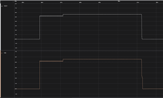
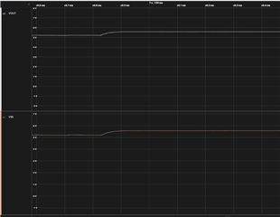
closeup view of VOUT insertion:
Here's a part of my schematic with test condition notes: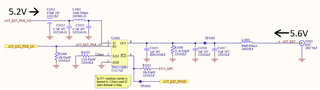
Visual look of the IC: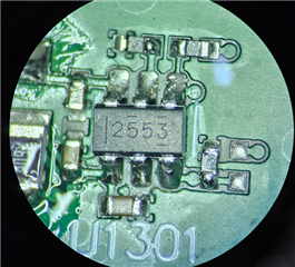
Any thoughts what might be an issue with this design are very appreciated
Thanks in advance
Yury

