This thread has been locked.

If you have a related question, please click the "Ask a related question" button in the top right corner. The newly created question will be automatically linked to this question.

TPS65219: Schematics Review

Part Number: TPS65219
Other Parts Discussed in Thread: AM6442,

Tool/software:

Hi TI team,
Greetings from VVDN Technologies.

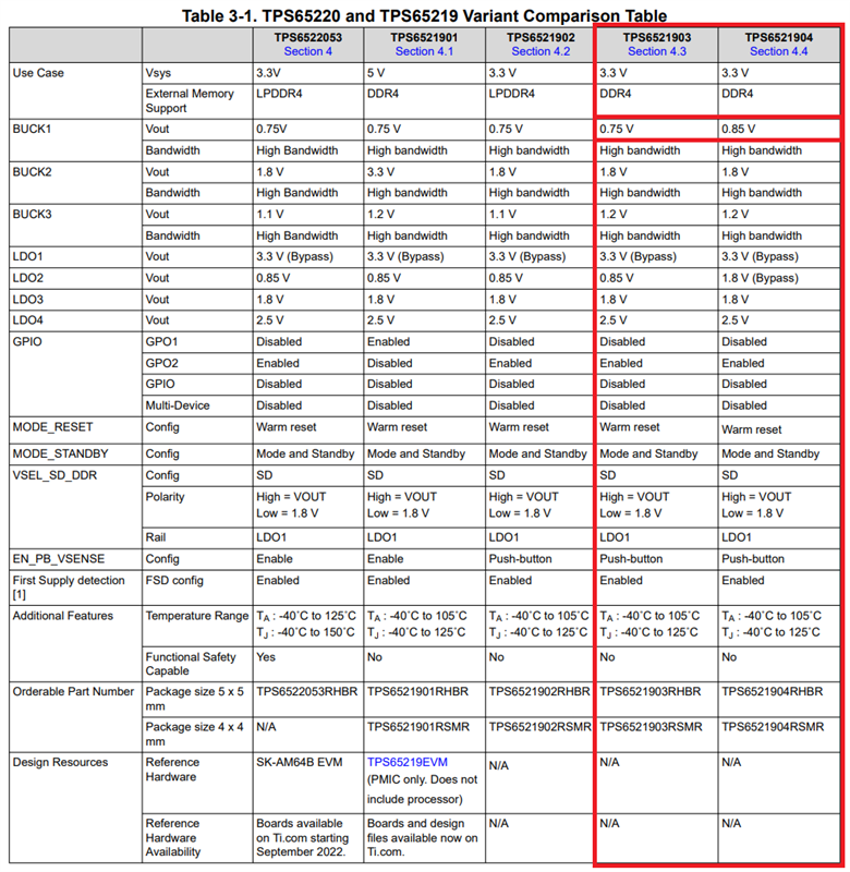
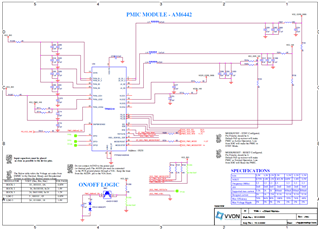
In our ongoing project we are using AM6442 Processor. Power solution for this one we are considering a PMIC with 7 Outputs ( 3 Buck and 4 LDO's). 

PMIC Details:
MPN - PTPS6521903RHBR
Desc - IC, TPS65219, PMIC, 7 Outputs, 3-DC/DC & 4-LDOs, VQFN-32
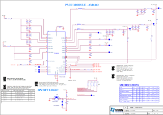
Please find the below attached schematics of PMIC and Provide your valuable feedback. 


With Best Regards,
Teja.

  • Hi Teja,

    Our standard time for schematic review is 1 week. I will review and provide my feedback by next Tuesday.

    In the meantime, can you please fill out this schematic checklist to make sure no small detail is missed.

    https://www.ti.com/lit/zip/slvafe2

    Sathish

  • Hi Sathish,
    Good day.

    Please find the below attached link for the Schematic check list sheet. I had filled all the inputs and cross verified with the schematics as well. Refer the filled values and provide the valuable feedback.

    Drive-Link

    Also While going through the datasheet which was revised recently on feb - 2025. previously we had used this PMIC part and at that time the manufacturing part number was PTPS6521903RHBR and in the current revised version MPN is TPS6521903RHBR.
    The only change I had noticed is the prefix - P was missing. 

    Please let me know is there any changes wrt hardware or any properties of the device with the new part number.

    Best Regards,
    Teja.

  • Hi Teja,

    I can not access google sheets, can you please attach it to the post?

    I reviewed the schematic and here is my feedback,

    - I see LDO1 and 4 are not sued, but since these are part of the sequence, it requires the output capacitance, otherwise PMIC will not power up.

    - In this 03 version of the device, Buck1 output voltage is defined as 0.75V, schematic shows 0.85V please check.

    -  In this version, all 3 Bucks are defined in High Bandwidth config and requires min. of 80uF capacitance. I suggest adding another 47uF to Buck2 and 3 outputs

    - Buck2 output is labeled as VCC_1V8 but PVIN_LDO2 labeled as VCC_PMIC_1V8, please check

    - check ON/OFF logic. PMIC_AM6442_EN need to be pulled high for normal operation and other end of push button need to be connected to GND.

  • Teja,

    A 'P' in the front of the device name indicates it is a pre-production sample and once the device is released to production, 'P' marking will be removed.

    Sathish

  • Hi Sathish,

    Thanks for the schematic review comments and the part number confirmation.
    Here by attaching the Updated schematics with the review comments considered.

    --> You had mentioned that for this 03 version of the device, Buck1 output voltage is defined as 0.75V. As per my knowledge we can configure the output voltage of Buck regulators. Since this PMIC had NVM in it either it can be factory programmable or we can configure it through Software. Please confirm this.

    Also please find the below attached Schematic checklist excel.

    8233.TPS65219 Schematic, Layout Checklist.xlsx

    With Best Regards,
    Teja.

  • Hi Teja,

    correct, you can change the default rail voltages after PMIC powers up but they will go back to default NVM values on any power cycle. Just need to write to PMIC after every power cycle.

    Check list comments showed VSEL is used for DDR but NVM is configured for SD, please check

    GPO2 is enabled in NVM and is part of the sequence, can you add a pull up to 3V3?

    Sathish

  • Hi sathish,

    Thanks for confirming the PMIC power Outputs.

    My query in the fixed outputs is, can we factory program this PMIC so that it can give only 0.85V all the time irrespective of any power cycles of PMIC. I completely agree that we can change the output values through I2C but, it will be better if we have a default factory programmed output of 0.85V. Please confirm this.

    VSEL_SD/VSEL_DDR pin is used for DDR, There is a configuration of VSEL pin if we leave the VSEL_DDR pin floating it will be configured as 1.2V. As we are using DDR4 1.2V is required. Configuration of SD or DDR can be done by MFP_1_CONFIG Register right.

    GPO2 pullup to 3V3 using 10K - Considered and implemented in scheme.


    Best regards,
    Teja.


  • Hi Teja, 

    Sathish is currently out of office, I will help to provide support in the meantime. 

    On the first startup, the TPS6521903 PMIC will output 0.75V by default. In order to reprogram, I2C communication has to be established with the device for the 0.85 voltage level to be programmed as the new default value. After that, then after any power cycle it will default to 0.85V, but the first initial startup will be 0.75V.

    A better option would be to switch to the TPS6521904 device, which has most all the same settings as TPS6521903, with BUCK1 set to 0.85V instead of 0.75V.
    This should be the best fit for your application.  

    Regarding the VSEL SD/DDR pin:

    By TPS6521903/04 default settings, VSEL_SD/VSEL_DDR pin is set to SD (VSEL_DDR_SD = 0x1, configured as SD). 
    Yes, configuration can be adjusted with MFP_1_CONFIG register, 
    But there should be no need to configure VSEL to DDR to set BUCK3, since Buck3 output is already set to 1.2 V by default. 

    Leaving as SD will only effect LDO1, which is not being used in your design. This should not effect anything. 

    I also noted that VSEL pin is tied to GND, not floating. This will also be fine since Buck3_VSET = 1.2 V..
    Or in SD configuration, LDO = 1.8 V (unused)

    Let me know if I can help clarify anything further. 

    Best Regards, 
    Sarah

  • Hi Sarah,

    Thanks for the confirmation on using TPS6521904/04 and Confirmation on the VSEL pin.
    No need of further clarification.

    Best regards,
    Teja.