This thread has been locked.

If you have a related question, please click the "Ask a related question" button in the top right corner. The newly created question will be automatically linked to this question.

UCC28950: Transformer Coupled Gate Drive - Calculation of Coupling Capacitor

Part Number: UCC28950

Tool/software:

Hello, 

After I go over the circuit diagram given in UCC28950 regarding the gate drive circuitry there, then read ''Fundamentals of MOSFET and IGBT Gate Driver Circuits'' written by Laszlo Balogh .

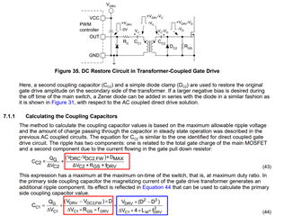
In this document there is a part to calculate the coupling capacitor in section of ''DC Restore Circuit in Transformer-Coupled Gate Drive''. I saw I couple things that I couldn't grasp the idea behind it. Which are as follow :

To calculate the value of Cc1 and Cc2, ripple voltage and the amount of charge passing through the capacitor in steady state is base. That is okay. So I have no issue with the calculation of Cc2 and I understand  how the equations of Cc2 is formed. I put a red box somewhere in the calculation, I will explain it later..

Now when we come the calculation of Cc1, the calculations given in the red box for Cc2 is exactly same. However the Cc1 is placed on the primary side and the red box calculation includes the secondary side diode and pulse peaks different between primary and secondary. So why is the same calculation given in red box applied for both Cc1 and Cc2 eventhough the Cc1 is on the primary side ? 

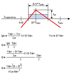
My second point is there is statement which is ''In the primary side coupling capacitor the magnetizing current of the gate drive transformer generates an additional ripple component''. I am also agree with that. The blue box given in the Cc1 calculation is related to this sentence, however there is no explanation about how to generate the equation given in blue box.  Could you help me to understand how to derive the expression given in blue box ?

Thank you 

Best regards

  • Hello,


    Could you send me a link to the paper you are referring too?


    Regards,

  • Hello Sir,

    Here is the link : https://www.ti.com/lit/ml/slua618a/slua618a.pdf?ts=1747037572721 ,page 41.

    Best Regards

  • Burak,

    Can you please clarify what exactly you are trying to achieve here? I noticed that you have another post asking a related topic. If you want to design a gate driver using transformer, there are many materials you can find online. This forum is more focused on TI parts.

    Thanks

  • Hello Sir,

    The topic is actually related to the couplig capacitor of UCC28950, the UCC28950 has same coupling capacitor and it does not include how to calculate the coupling capacitor so I go over another paper published by TI as well about mosfet gate drive. This paper include same structure given in the UCC28950.  So I saw a couple of points regarding the calculation of coupling capacitor and I just wanted to ask them. If I did any mistake regarding the question, I apologize but I thought that the topic is still connected to the design of UCC28950.

    I am generally not asking how to design the gate drive from the beginning, I am mostly asking the specific parts of the design as in the previous and current question. For example in this question instead of memorising the equation given the paper, first I tried to understand where does it come from and I know most idea behind the the equations so I asked the small points where I couldn't match with what I know. 

    Best regards

  • Hi There,

    Let me try to answer your questions:

    1) The expressions in the red boxes must be the same, except deltaVc1 vs. deltaVc2 obviously. The remaining parts of the equation is the charge passing through the capacitors. Based on the secondary circuit we define the charge going through Cc2. The same charge goes through the secondary and primary windings of the transformer (1:1 gate drive transformer), consequently the coupling capacitor Cc1 on the primary. I hope you see this now and understand why the expressions are identical.

    2) I tried to locate the original derivation but I wrote this article so long ago, I couldn't locate it. So I derived the charge for you again. It seems that I might have made a mistake in the original article or I defined some of the variables differently based on the application I had for the example. I am confident that my derivation is correct now, the 2*D multiplier difference is circuit dependent. (double ended converters would have a 2*D multiplier difference).

    Based on this derivation you can also derive your own relationship and magnetizing inductance impact. The blue rectangle represents the charge we are looking for. That extra charge passes through Cc1 due to the magnetizing current contribution. I hope this is clear now as well.

    Regards,

    Laszlo

  • Hello Sir,

    Firstly, I am a very big fan of yours and your studies, thank you for your answer sir.

    I got the point but have a small question ; Ipeak is actually based on the original drive signal so we calculated the magnetising current based on this. Then due to  capacitor, our signal will have positive and negative peaks. Since Vc= 0.5xVdrive , we should divide the Ipeak by 2 , and divide the Tdrive by 2 as well . Am I thinking correct sir?

    Thank you 

    Best Regards

  • In my derivation you can recognize that I peak is just the peak of the magnetizing current. We only calculate the magnetizing current contribution to the ripple voltage in this case and use superposition to add it to the other effects. Its expression (Ipk=) already has the 0.5 multiplier (0.5*D*Tdrv) which yields half of the delta current (Im goes from -Ipk to +Ipk). I hope you can follow this on the drawing of the waveform I included. For the charge calculation (Q=Ipk/2 * Tdrv/2) I included the 1/2 factor for Ipk and the 1/2 factor for half of the Tdrv to arrive to the area of the blue rectangle (the charge we are looking for) in the waveform drawing.

    I do not think that I would have left anything out.

    Regards, Laszlo

  • Ohh, okay it is more clear now. I understood fully now. I misinterpreted the graph.

    Thank you so much for your explanations

    I work hard, hoping one day to be a professional like you sir.

    Thank you 

    Best regards