This thread has been locked.

If you have a related question, please click the "Ask a related question" button in the top right corner. The newly created question will be automatically linked to this question.

TPS25730: TPS25730DREFR

Part Number: TPS25730
Other Parts Discussed in Thread: TPD2S300, TPD4S311A,

Tool/software:

Hello Team,

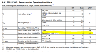
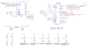
I our design we are planning to implement TPS25730DREFR IC in our design for Sink only PD application (NO BATTERY, Only Plug and Play application with indication over the GPIO of the IC) used in the device.

I would Like to know about Purpose of VIN_3V3 Pin !

In our device We are not going to use any Battery .It would be just Plug and Play application.

If we leave VIN_3V3 pin unused/Floating would there be any impact ?

Regards,

Tirthal Patel

  • Hi Tirthal,

    VIN3V3 is used for IC power when the IC is powered by the system (internal power).

    If you only intend on using power from VBUS and VIN_3V3 is unused, please Bypass the pin with the CVIN3V3 capacitance. The pin can be left unused and there should be no impact other than the IC being disabled if a USB-C source is not connected to the port.

    Thanks and Regards,

    Chris

  • Hey Christopher ,

    Also I would like to know what is the max current LDO_3V3 & LDO_1V5 can provide !

    If we are operating the IC from the VBUS Power then also we would be getting output on the LDO_3V3 and LDO_1V5 Correct ?

    What should be the status of the below mentioned pins, Do they require any pullup/pulldown : 

    Pin 6 : CAP_MIS

    Pin 13 : PLUG_FLIP

    PIN 10 : DBG_ACC

    Pin 18 : FAULT_IN_N

    Pin 19 : SINK_EN_N

    PIN 37 : PLUG_EVENT

    Regards,

    Tirthal Patel

  • Hi Tirthal,

    We do not recommend using LDO_1V5 for powering any peripherals. The pin exists for adding the capacitance.

    For LDO3V3, it is only intended to be used for the GPIO and I2C pullup resistors required by the TPS25730. It can also be used to power a CC-line protection device like the TPD2s300 and TPD4s311A. You should not be powering much else from LDO3V3.

    Please see the DS for more information on the GPIOs.

    Any output, open-drain GPIOs need a pullup resistor to LDO3V3 when used. They can be floating if unused.

    The Fault_In pin should be pulled up to LDO3V3 through a 10k resistor when used or unused to ensure it is pulled high.

    Thanks and Regards,

    Chris

  • Hi Christopher,

    Can you please check the above design,

    Things I would like to share as mentioned below : 

    1.Pin 36, VIN_3V3 is provided with Bypass Cap.

    2.Pin 1 & 4 , LDO_3V3 & LDO_1V5 share the same Value 10UF Bypass capacitance.

    3.Pin 19, SINK_EN_N This Pin is Pulled Down ,to maintain constant sink configuration when USB-C is Plugged IN.

    4.Pin 6, CAP_MIS What is the exact use of this pin does it require any controlling ,currently Pull-Down is provided on this pin.

    5.Pin 10, Debugg_ACC What is the exact use of this pin ,currently Pull-Up is provided on this pin.

    Please help me on the above raised query !

    Regards,

    Tirthal Patel


  • Hi Tirthal,

    1. This is fine
    2. This is fine
    3. Sink_EN_N is an open drain output. It does not need to be pulled down low. You should leave it pulled up to LDO3V3, not pulled low. This just indicates if the sink path is enabled. It defeats the purpose of the pin to tie it to GND through a resistor.
    4. All open drain outputs should either be pulled up to LDO3V3 or left floating. CAP_MIS should not be pulled down. 
      1. It indicates if a caps mismatch event has occured. This will occur if the USB-C PD source advertises a max power less than the power required by the minimum voltage and operating current.
      1. This indicates if the connected device is a Debug accessory.

    The CC lines should have 330pF of filtering capacitance on each line.

    As mentioned earlier, If the pin is an open drain output, it should either be pulled up to LDO3V3 through a pullup resistor, or left floating if unused. If they are outputs, they do not require any controlling and are intended to indicate connection status.

    Thanks and Regards,

    Chris

  • Hi Christopher ,

    We have updated the design can you please review it ,Also attaching the BOM for the same.

    Can you let me know how VCONN is going to get power supply, I am not able to find block diagram in the data sheet ,Will the IC internally provide the VCONN supply from the CC1/CC2 pins ??

    USB PD CONTROLLER.xlsx

    Regards,

    Tirthal Patel

  • Hi Tirthal,

    The TPS25730 does not support VCONN, which is only needed for source applications and data applications. The TPS25730 is meant to be a barrel jack replacement that only support the sink power role.

    I primarily reviewed the changes requested in the last thread, everything recommended their looks fixed now.

    For pins 26,27, and 36. You can tie these directly to ground, they do not need 10k pulldowns.

    The VBUS node (anything connected between the VBUS pin of the type-c connector and the VBUS pins of the TPS25730) should have max 10uF cap. It seems like you have more than 34.7uF between C51, C77, C78, and C56, not including all the other caps you have on the bus. The total cap must be 10uF max which is defined by the USB-C PD spec for sinking ports.

    The schematic looks good otherwise.

    Thanks and Regards,

    Chris

  • Hi Christopher,

    I have updated the design for the VBUS (Between Connector and IC) which is well under 10Uf.

    Let me know your feedback!

    Regards,

    Tirthal Patel

  • Hi Tirthal,

    Just to clarify, the C59,C60,C61,C62, and C54 caps to "place near the pins"  should be placed near the J2 connector VBUS pins. The recommendation is for the connector VBUS pins, not the PD controller PD pins. As long as the 4.7uF is near the TPS25730, it should be fine.

    VBUS Cap looks better now, but you still have >10 (14.7uF with C56 and C51). We still recommend it stays under 10uF.

    Thanks and Regards,

    Chris

  • Hi Chris,

    In the design previously C51 was 10uF which was DNP ,which I have updated to 4.7uF Mounted.

    Also now the overall capacitance on the VBUS line is <10uF (C51 & C56 9.4uF).

    Also updated the placement of C59,C60,C61,C62, and C54 near to the connector J2.

    Regards,

    Tirthal Patel

  • Hi Tirthal,

    In the design previously C51 was 10uF which was DNP ,which I have updated to 4.7uF Mounted.

    Ok, yeah I missed the DNP marking. You should be good now.

    Thanks and Regards,

    Chris

  • Thank you for the prompt response .!!

    Regards,

    Tirthal Patel