This thread has been locked.

If you have a related question, please click the "Ask a related question" button in the top right corner. The newly created question will be automatically linked to this question.

TPS23755: Design/schematic review

Part Number: TPS23755

Tool/software:

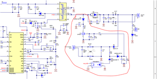
Attached is a modified version of TPS23755EVM-894. 

I made some parts changes to reduce BOM veriety.

Designed for dual input with seamless transition. Adapter as primary.

LED and LED resistors act as load for PoE while adapter is on.

Does schematic look okay? Do you see any glaring issues?

If I change D1 to a higher value, can the system use 24 adapter input?

tps23755-2.pdf

  • TI-US is closed today. Please allow a delayed response to your query.

  • Hi Derik,

    Thanks for reaching out!

    1. D18 is recommended to be mounted 

    2. C112 is better to be a electrolytic cap

    3. D4 and D3 recommended >3A Schottky diode 

    4. For seamless transition, the current 2nd side dummy load maintain power signature circuit could be not working. You can refer the EVM if you need 

    5. The 2nd adapter voltage better to be the same or very close to the PoE 12V output for oring application. 24V may need to do a voltage step down.

    Best regards,

    Diang