This thread has been locked.

If you have a related question, please click the "Ask a related question" button in the top right corner. The newly created question will be automatically linked to this question.

BQ25756: Charging not starting with no fault or error

Part Number: BQ25756
Other Parts Discussed in Thread: BQ25750, , BQSTUDIO, EV2400

Tool/software:

Hello,
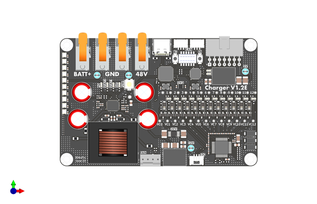
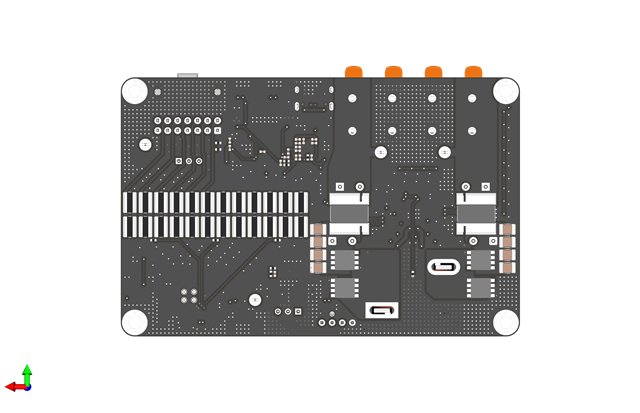
We have developed a new version of our Charger that uses larger MOSFETs than before and (as we believe) features an improved layout. Unfortunately, the new design is not functioning at all.
The problem:


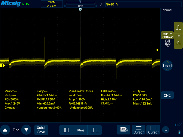
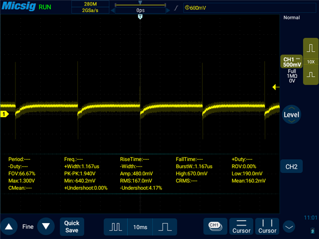
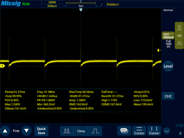
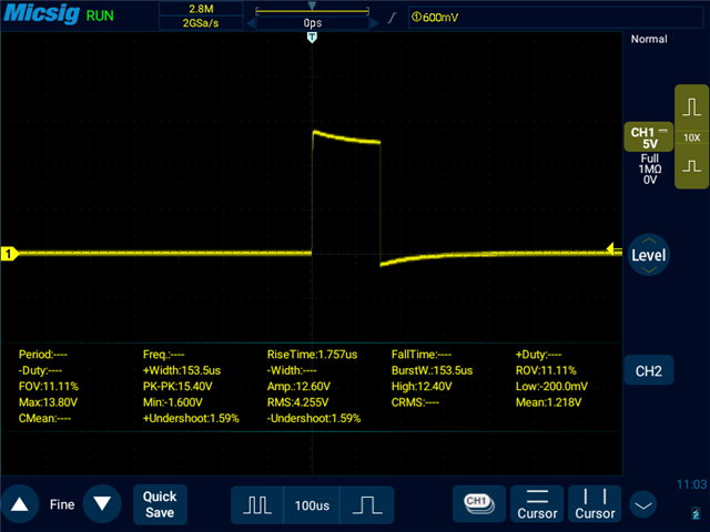
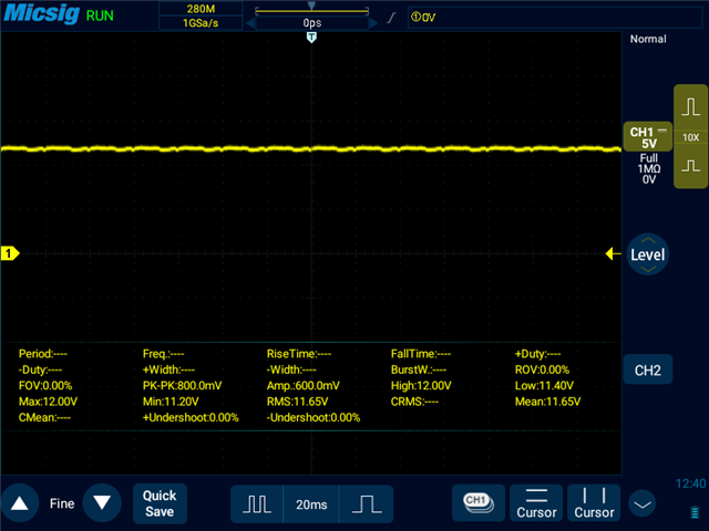
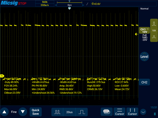
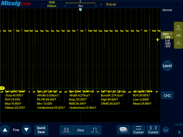
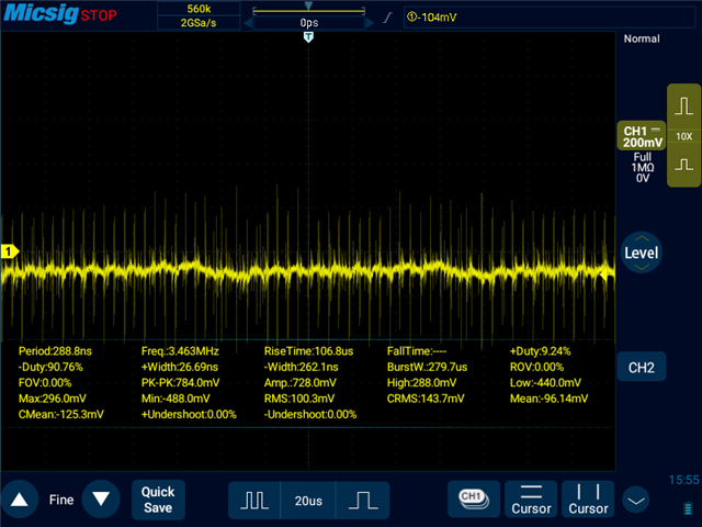
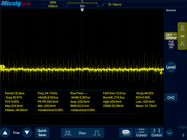
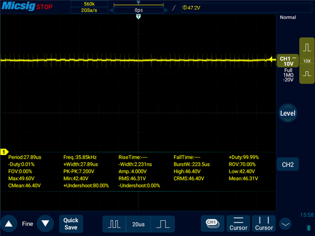
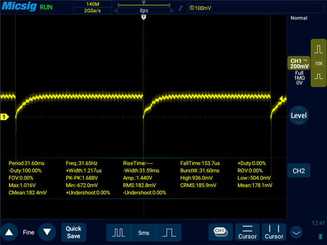
The INT pin is periodically pulled low at approximately 32 Hz for short pulses.
 ChargerGUI reports no faults or errors.
 No current is flowing through the board.
 The low-side MOSFETs appear to switch correctly: the gate voltage shows a clean digital signal with good rise and fall times and no ringing.
However, the high-side MOSFETs are not switching properly — the gate voltage rises slightly but then quickly stops. (Screenshots are attached.)

What we have tested so far:
* Increased dead time to maximum and various random values between max and min → no change.
* Increased bootstrap capacitors from 100 nF to 470 nF, then to 1 µF → no change.
* Verified that gate driver strength is set to ‘fastest’.
* Verified that switching frequency (fsw) is set to 200 kHz.
* Disabled temperature sensor using ‘EN_TS’.
* Enabled ‘DIS_CE_PIN’.


In the ‘Status & Faults’ tab, only the ‘FSW_SYNC_FLAG’ is green; all others are off.
Previously, we used the SIR880BDP-T1-RE3 MOSFETs. Now, we are using the IAUT165N08S5N029ATMA2 and the FDBL86366-F085 on two otherwise identical boards. Both exhibit the same behavior.

High side MOSFET gates (both show identical pattern):

High side mosfet gates

Low side MOSFET gates (both show identical pattern):

low side mosfet gate


Any help diagnosing this issue would be highly appreciated.


Thanks,

Max

  • Hello Max,

    Thanks for working on this.

    I've got a few questions to help debug this:

    • What's the voltage on REGN, DRV_SUP, and the BTST Caps?
    • Does the circuit work if you use the SiR880BDP FETs? It might be hard to solder the FETs onto the board though.
    • Are you using an external gate drive voltage? If so, does going to a higher external gate drive of 10V or so improve the behavior of the circuit?

    Best Regards,
    Ethan Galloway

  • Hi Ethan,


    thanks for following up. Here are the answers to your questions:


    1. Voltages on REGN, DRV_SUP, and BTST caps:
    - REGN was measured at 5 V.
    - DRV_SUP is externally supplied with a stable 12 V from a Wurth Elektronik 173951275.
    - Both BTST1 - SW1 and BTST2 - SW2 measure around 11.5 - 11.7 V, with moderate ripple (~400 - 700 mV). The bootstrap capacitors appear to charge correctly.


    2. Does the circuit work with SiR880BDP FETs?
    - The previous board revision using SiR880DP FETs worked, but had overheating issues.
    - The current boards use IAUT165N08S5N029, which have significantly different/larger footprint. Using the old mosfets seems really hard to me and I would like to avoid trying that if it is not the last way of proceeding. I also suspect the larger gate charge could be overloading the internal gate drivers, especially since we currently use 0 Ω gate resistors. I am unsure if larger gate resistors would help, as this also further increases the switching time?


    3. Are you using an external gate drive voltage?
    - Yes, we are feeding DRV_SUP externally with 12 V instead of using the internal source. I think that is the highest we can safely attach to this pin.


    Let me know if you'd like additional scope captures or more infos/screenshots of some registers.


    Best regards,


    Max

  • Hello Maximilian,

    Thanks for the new information.

    I also suspect the larger gate charge could be overloading the internal gate drivers, especially since we currently use 0 Ω gate resistors. I am unsure if larger gate resistors would help, as this also further increases the switching time?

    I'm not sure if the gate resistors would help either. By the way, there is a limit to the switch node capacitance for the charger though. In the datasheet, we recommend a C(SW) to be less than 160/VIN. I've copied the relevant part of the datasheet below:

    From this, I think the parasitic capacitance of the FDBL86366−F085 might be too high to work with the BQ25750.

    I have a few questions to help us debug this:

    • Can you take an oscilloscope capture of SW1, SW2, LODRV1, and HIDRV1 while the circuit is in buck mode? I want to see how SW1 and SW2 are being affected by the gate drive waveforms.
    • If possible, can you take an oscilloscope screen shot of BTST - SW? This may tell us if the BTST capacitor voltage is browning out.
    • Can you send me the register file? It would be good to check what mode the charger thinks it's in.

    Best Regards,
    Ethan Galloway

  • Hi Ethan,

    here are my measurements, all done with the IAUT165N08S5N029.
    VAC was ~47528mV and VBAT was ~45350mV.

    SW1 - GND

    SW2 - GND

    HIDRV1 - GND

    LODRV1 - GND

    BTSTS1 - SW1

    BTST2 - SW2

    Register file charging enabled:

    regs(5).json.zip

    Schematic:

    I'm not sure if the gate resistors would help either.

    Should I try 10-20Ω gate resistors or rather not?

    Kind Regards,

    Max

  • Hello Max,

    That's strange. It looks like BTST has enough voltage to drive HIDRV, but HIDRV won't turn-on. LODRV seems capable of switching though.

    I'm curious if the circuit will work in boost mode. If you lower the input voltage below VBAT, does the circuit work then?

    On that note, if you have a 20V input to 10V battery, does the circuit charge then?

    Best Regards,
    Ethan Galloway

  • Hi Ethan,

    I’ve made good progress getting the BQ25756-based charger up and running. The initial startup issue was caused by an MLCC capacitor on the FSW pin. Apparently, the chip interpreted this as a request for an external sync signal instead of a resistive frequency setting, which caused HIDRV to remain inactive. After removing the capacitor, the charger started working correctly.

    With a heatsink in place, I was able to run 19.6 A continuous charging at 40 V output without issue.

    However, a new critical issue appears at higher output voltages around 45 to 46 V. The charge current becomes unstable and fluctuates rapidly, even though the target is fixed at 20 A. At the same time, the VAC_DPM_FLAG is being triggered. The VAC_DPM threshold is set to the minimum value of 4.2 V, and I’ve confirmed with a scope measuring directly at the VAC pin of the IC that the voltage never drops below 44 V. I can’t explain why the DPM flag is being set in this condition. This is currently the most important issue for me to understand and resolve, as the current instability seems to correlate directly with this flag and may also explain the remaining thermal problems.

    As a secondary point, we previously used Würth 74439370047 (4.7 µH, SMD) inductors, which saturate around 20 A. They actually performed quite well thermally at 40 V and 20 A, reaching only about 52 °C, so DCR is likely not the limiting factor. However, at higher output voltages the thermal performance degraded significantly, which appears to be related to saturation and high duty cycle conditions.

    We replaced them with Würth 74437625201002 (10 µH, THT), which have a significantly higher saturation current of around 30 A and only slightly more inductance. These new inductors still reach over 100 °C during testing at higher voltages, but since the main issue is the unstable current and DPM behavior, I believe the inductor heating is more a symptom than the cause.

    I would really appreciate your advice regarding why VAC_DPM_FLAG might be triggered in this setup, despite the input voltage being steady and far above the configured threshold. Any additional suggestions to improve stability and eliminate these current oscillations at high output power would be very welcome.

    Best regards,
    Max

  • Hello Maximilian,

    I would not have expected an MLCC capacitor on FSW to cause that issue. Thanks for finding this out and letting me know about this.

    I've got a few questions to help debug this:

    • Does the charger's behavior improve if you set the bit EN_CONV_FAST_TRANSIENT=0?
    • Does the oscillation go away if you put more capacitance on VIN and VBAT? You might be able to quickly test this by putting a 1000µF in parallel with VBAT.
    • Does this behavior happen when the circuit is in buck-boost mode?
    • If possible, can you measure the waveforms of SW1, SW2, IBAT, and VBAT?

    Best Regards,
    Ethan Galloway

  • Hi Ethan,

    the issues are almost solved now. The instability apparently simply resulted from too little inductance. After mounting 2 10uH Inductors in series the issue is almost gone. Now, with 48V input and 46V output and demanded 20A charging current (that is the worst case I found) I get charging current fluctuating from 17-18A at ~0.5-1Hz. That is still not amazing, but for now fine for me. 

    How do you recommend tuning the switching dead time? I am afraid of burning something by doing just trial and error. Currently I am running at highest dead time. 

    I will try to capture the waveforms tomorrow, maybe we can figure out the reason for the remaining oscillations. 

    I only found the bit EN_CONV_FAST_TRANSIENT as a readable bit:


    Does this behavior happen when the circuit is in buck-boost mode?

    The behaviour is worst at 46V out and 48V in. But it appears roughly from 45.5-49V output at constant 48V input. I think it is the region where the charger switches from buck to boost and where duty cycles are highest and therefore hardest to properly control. 

    Kind Regards,

    Max

  • Hello Max,

    the issues are almost solved now. The instability apparently simply resulted from too little inductance.

    That's great to hear.  You might also want to try increasing the inductor's DCR. The charger detects the inductor's DCR when charging starts and increasing the DCR may help improve the charger's stability.

    How do you recommend tuning the switching dead time?

    I would recommend on zooming on the MOSFET gate voltages. I think that will give you a good idea of what the allowable dead time will be.

    The behaviour is worst at 46V out and 48V in. But it appears roughly from 45.5-49V output at constant 48V input. I think it is the region where the charger switches from buck to boost and where duty cycles are highest and therefore hardest to properly control

    This is true for the BQ25756.

    Some of the instability might be caused from the battery load though. Can you tell me what you are using for the load on VBAT? I know some of my e-loads start causing instability in the output current when the e-loads reach their own current limits.

    Best Regards,
    Ethan Galloway

  • Hi Ethan,

    here are the additional signals:

    SW1 - GND @ 20A

    SW1 - GND @ 10A

    SW2 - GND @ 20A

    SW2 - GND @ 10A

    IBAT (SRN - SRP) @ 20A

    IBAT (SRN - SRP) @ 10A

    VBAT @20A (measured at BAT connectors of PCB)

    Some of the instability might be caused from the battery load though. Can you tell me what you are using for the load on VBAT? I know some of my e-loads start causing instability in the output current when the e-loads reach their own current limits.

    I am using a EA PSB 10080-60 bidirectional DC powersupply. I thought of the same problem and also testet wit a big 12S LiIon pack which showed the same fluctuations. 

    Kind Regards,

    Max

  • Hello Max,

    Thanks for the new information and the new tests.

    I am using a EA PSB 10080-60 bidirectional DC powersupply. I thought of the same problem and also testet wit a big 12S LiIon pack which showed the same fluctuations. 

    Ah, thanks for the clarification.

    I only found the bit EN_CONV_FAST_TRANSIENT as a readable bit:

    I see that TI charger GUI doesn't let you write to this bit. Is there any chance you have access to a microcontroller or an EV2400 to use BQSTUDIO to write to this bit?

    Also, I'll have to update the BQ25756 in TI CHARGER GUI to allow for this bit to be written. I'll try to get this done soon. At most, I should be able to get this done before the end of the month.

    For your oscilloscope images, I'm seeing a lot of overshoot. Just to be sure, are you connecting the ground leads of the probes to the PCB's ground? This will reduce the inductance of the GND loop and reduce the ringing on the signals.

    Best Regards,
    Ethan Galloway

  • Hi Ethan,

    Just to be sure, are you connecting the ground leads of the probes to the PCB's ground?

    For the SW measurements I connected GND and SW to testloops directly connected with copper pours and close to MOSFETs.

    For shunt measurements I connected short wire stubs to the MLCC closest to the IC and between the two shunt measurement pins on each side of the IC. 

    Is there any chance you have access to a microcontroller or an EV2400 to use BQSTUDIO to write to this bit?

    We want to control the BQ25756 with an ESP32S3 in the future and currently are writing code to do so. When we have a working state, we can try setting the bit with this. 

    Kind Regards,

    Max

  • Hello Max,

    Thanks for the update.

    By the way, I started the update process for BQ25756's TI Charger GUI to allow writing to the EN_CONV_FAST_TRANSIENT bit. I'll try to let you know when this completes.

    For the SW measurements I connected GND and SW to testloops directly connected with copper pours and close to MOSFETs.

    For shunt measurements I connected short wire stubs to the MLCC closest to the IC and between the two shunt measurement pins on each side of the IC. 

    These sound like good measurements. In that case, you may want to set the oscilloscope bandwidth filters to 20MHz or around that area. This will help clean up the oscilloscope display. Signals above 20MHz don't really affect the circuit that much.

    We want to control the BQ25756 with an ESP32S3 in the future and currently are writing code to do so

    Let me know if you want driver code or examples for this.

    You've probably already tried this, but since you have improved the charger's inductors, does putting a larger cap on VBAT improve the performance? This might reduce the ripple on VBAT.

    Best Regards,
    Ethan Galloway

  • Hello Max,

    The edits to the BQ25756's TI Charger GUI are complete. You should be able to use this GUI to edit the EN_CONV_FAST_TRANSIENT bit now.

    Let me know if you have any questions about this.

    Best Regards,
    Ethan Galloway

  • Hi Ethan, 

    In that case, you may want to set the oscilloscope bandwidth filters to 20MHz or around that area. This will help clean up the oscilloscope display

    I was not able to do any of this so far.

    We faced issues again. I was able to get rid of all the previous issues with fluctuating current just by adding another inductor last week. So we had 30uH in total, which seems super excessive to me. We were able to charge with 20A (~19.2A in reality) in all voltage regions. Today we tested again and it is barely working. No changes to the hardware were made. We noticed that the chargerGUI received an update, because we were unable to load our old JSON files for configuration. But after setting all variables manually, we started having issues.

    Also, did you change the IAC_DPM settings? Before we set the limit to 50A, now only 20A are possible. We are still using a 2mOhm shunt on the input and 5mOhm at the battery side. Is this a correct setup?

    When we want to charge with 48V VAC and 42-49V VBAT, the current is all over the place. For testing, we always just enabled and disabled charging at ~5-10s intervals and observed the charge current. Sometimes the current is fluctuating between 17-18A, sometimes 13-14A, sometimes we get the 19.2A, and most of the times it "charges" super stable at 1.4A even though we request 20A. When we start at 41V and raise the voltage slowly up to 50V, the problem is completely gone. It charges completely normal at 19.2A throughout all VBAT voltages. 

    When we tried charging only at 10A, the issue appeared to be happening fewer times, but quite often after a few seconds of runtime, we were able to hear weird cracking and hissing noises. We tried to find the source, but could not find any broken components. 

    Do you think the very noisy shunt measurements are messing with the current control? If yes, why is the device often stuck at this weird 1.4A point? What would you recommend doing to reduce the noise? Add MLCCs with smaller capacitance or higher, or both? 

    Best Regards,

    Max

  • Hello Max,

    . We noticed that the chargerGUI received an update, because we were unable to load our old JSON files for configuration. But after setting all variables manually, we started having issues.

    Ah, sorry about this. This is probably due to the update. I think a new JSON file created with the new TI Charger GUI should work.

    Also, did you change the IAC_DPM settings? Before we set the limit to 50A, now only 20A are possible. We are still using a 2mOhm shunt on the input and 5mOhm at the battery side. Is this a correct setup?

    The IAC_DPM register range was changed to use a 5mΩ sense resistor (This is the default on the EVM). A 2mΩ IAC sense resistor will still work with the GUI. To find the adjusted current setting, multiply the desired input current limit by 2/5. For example, to get a 10A current limit from a 2mΩ sense resistor, the IAC register will need to be set to 4A.

    Let me know if you have any questions about this.

    When we want to charge with 48V VAC and 42-49V VBAT, the current is all over the place. For testing, we always just enabled and disabled charging at ~5-10s intervals and observed the charge current. Sometimes the current is fluctuating between 17-18A, sometimes 13-14A, sometimes we get the 19.2A, and most of the times it "charges" super stable at 1.4A even though we request 20A. When we start at 41V and raise the voltage slowly up to 50V, the problem is completely gone. It charges completely normal at 19.2A throughout all VBAT voltages. 

    Does setting EN_CONV_FAST_TRANSIENT=0 help with this?

    Do you think the very noisy shunt measurements are messing with the current control?

    This is very possible. Can you measure the ACP and SRP pins with an oscilloscope to see how much noise is on those pins?

    Also, can you send me the layout for the board so I can review it?

    If yes, why is the device often stuck at this weird 1.4A point?

    That's a good question. I don't have enough information to determine this yet.

    What would you recommend doing to reduce the noise? Add MLCCs with smaller capacitance or higher, or both? 

    This will depend on the noise frequency. I think adding a large bulk capacitor (like ≈1000µF or so) to VAC and VBAT might be a good place to start to see if a bulk capacitor will stabilize the input and output.

    Best Regards,
    Ethan Galloway

  • Hi Ethan,

    The IAC_DPM register range was changed to use a 5mΩ sense resistor (This is the default on the EVM). A 2mΩ IAC sense resistor will still work with the GUI. To find the adjusted current setting, multiply the desired input current limit by 2/5. For example, to get a 10A current limit from a 2mΩ sense resistor, the IAC register will need to be set to 4A.

    I already thought that would be the case but wanted to be sure.

    Does setting EN_CONV_FAST_TRANSIENT=0 help with this?
    Can you measure the ACP and SRP pins with an oscilloscope to see how much noise is on those pins?

    I will be able to test this on monday. 

    Charger V1_1.zip

    In the meantime, here are my design files. V1_1 is what we are currently working on. Please note that we removed the SMD inductors and have now installed 3x 74437625201002 Wurth Elektronik inductors externally in series. Previously, we used only 2 of them. We increased to 3 because it allowed us to charge at 20A when we tested last week. This week, as already stated without changes to the hardware it is barely working at all. On monday I will also triple-check if we have the settings correct as we had to set them manually. Do you see any possibility how the update of the chargerGUI is causing this issue even when the settings are the same as before?

    This will depend on the noise frequency. I think adding a large bulk capacitor (like ≈1000µF or so) to VAC and VBAT might be a good place to start to see if a bulk capacitor will stabilize the input and output.

    I can and will also test this oon monday. We already have 4x 330uF (1320uF) on input and output. Do you think that is still not enough?

    I hope to give you all the measurements on monday evening. 

    I will measure at requested 20A the following signals - reference:
    ACP - ACN

    ACP - GND

    ACN - GND

    SRP - SRN

    SRP - GND

    SRN - GND

    If more/others would be helpfull please tell me. 

    Also instructions on wether it matters what actually happenes during those measurements regarding charging current would be nice. Does it matter if the measurements are from the same actual currents flowing? It is not very reproducible and therefore might be hard to ensure same testing situations for all measurements.

    Kind Regards,

    Max

  • Hello Max,

    Thanks for working on this.

    I'll look over your design files next week. I'll need to get Kicad installed on my laptop.

    For your inductors, do you see any change in the charger's behavior when you use an inductor with a higher DCR?

    Do you see any possibility how the update of the chargerGUI is causing this issue even when the settings are the same as before?

    No, I don't see how the update could have changed anything. I'll try to check just to make sure.

    We already have 4x 330uF (1320uF) on input and output. Do you think that is still not enough?

    This should be enough capacitance. Adding more capacitance might be good to check to see if that changes the charger's behavior.

    I recommend the following measurements:

    LODRV - GND (This signals will make sure that the FETs are being driven properly)

    HIDRV-SW

    SW1 - GND

    SW2 - GND

    BTST-SW (This will make sure HIDRV has enough power. If you see HIDRV working fine, you probably won't need to check this).

    ACP - ACN (You can also use a current probe to measure this)

    SRN-SRP (A current probe would also work here)

    ACN - GND (This will check if there's any weird spikes or dips on this signal. You only need to check this once)

    SRN - GND (This will check if there's any weird spikes or dips on this signal. You only need to check this once)

    DRV_SUP (This will make sure that DRV_SUP is enough. You only need to check this once)

    Also instructions on wether it matters what actually happenes during those measurements regarding charging current would be nice. Does it matter if the measurements are from the same actual currents flowing? It is not very reproducible and therefore might be hard to ensure same testing situations for all measurements.

    This is an understandable problem. Just let me know what the voltages and currents were when the waveforms were captured. Make sure to also note the register settings and if any register flags were set as well.

    Let me know if setting EN_CONV_FAST_TRANSIENT=0 improves the charger's behavior.

    Best Regards,
    Ethan Galloway

  • Hello Max,

    Just to let you know, I got Kicad working on my work computer. Thanks for being patient with the delay here. I'm not seeing any obvious issues in the layout, though. In fact, the layout looks really well done. I'll try take a closer look at the schematic next week

    Best Regards,
    Ethan Galloway

  • Hi Ethan,

    The issue seems resolved for now. It was caused by an unfortunate series of events.

    Last time, I added a third inductor and initially thought everything was working fine at 20A. In reality, the IBAT ADC had stopped functioning and always showed 0mA, likely due to damage during hot air soldering or some other mistake (I did not notice this on that day). Since the control loop was not receiving valid current feedback, it seems to have kept pushing current blindly, which happened to be around 20A at that moment.

    We then added the third inductor to a second board and started seeing the same problems. Looking back, the root cause seems to be a combination of noisy shunt measurements and too much inductance, or possibly more EMI due to the additional inductor placed close to the board.

    After switching to a board with a working IC, using only two inductors totaling 20 uH, and setting EN_CONV_FAST_TRANSIENT=0 (which made a big difference), we were able to control everything as expected and reach the 20A target.

    At the moment, the only minor issue is that the VBAT ADC reading is consistently about 0.5 V lower than the actual VBAT. Do you know whether the device uses the shunt pins or the FB pins for measuring VBAT ADC? Since the offset remains even when charging is disabled, I doubt it is caused by switching noise. If it is measured at the FB pins, the offset could be due to the resistor tolerances in the divider (I used 1% resistors).

    Unless you specifically need it, I would prefer to skip capturing oscilloscope data for now and save the time.

    I'm not seeing any obvious issues in the layout, though. In fact, the layout looks really well done.

    Do you think the shunt noise could be significantly reduced by changing the layout and using much shorter traces between the shunts and the IC? The downside would be that more of the high-current and high-temperature parts and traces would end up closer to the IC.My hope is, that with cleaner shunt measurements we can reduce the need for C and L. 

    I am thinking about something like this:

    I guess it's hard to say for sure, but I would appreciate your gut feeling on this. 

    Best regards,

    Max

  • Hello Max,

    Thanks for the update and the new information. I'm glad to hear this has been mostly resolved!

    Last time, I added a third inductor and initially thought everything was working fine at 20A. In reality, the IBAT ADC had stopped functioning and always showed 0mA, likely due to damage during hot air soldering or some other mistake (I did not notice this on that day). Since the control loop was not receiving valid current feedback, it seems to have kept pushing current blindly, which happened to be around 20A at that moment.

    It sounds like the SRN / SRP pins got damaged on this IC.

    After switching to a board with a working IC, using only two inductors totaling 20 uH, and setting EN_CONV_FAST_TRANSIENT=0 (which made a big difference), we were able to control everything as expected and reach the 20A target.

    I'm glad to hear that this worked.

    Do you know whether the device uses the shunt pins or the FB pins for measuring VBAT ADC?

    The IC uses the SRN/SRP pins to measure the VBAT ADC. The ADC is intended to be a general indicator and there's not an accuracy specification for the ADC.

    Unless you specifically need it, I would prefer to skip capturing oscilloscope data for now and save the time.

    Yeah, we don't need these measurements anymore.

    Do you think the shunt noise could be significantly reduced by changing the layout and using much shorter traces between the shunts and the IC?

    Let me think about this and get back to you. My gut feeling would be to not adjust the board if it's working. I think the decision to redo the layout would depend on your other systems needs. For example, do you need to adjust the cost by using smaller inductors or capacitors? Or, does the system need a smaller battery charging board?

    Also, you might be able to test how much capacitance is needed on the current board by slowing removing capacitance. This way, you can save on the cost of capacitors without having to do another board layout.

    Best Regards,
    Ethan Galloway

  • Hi Ethan,

    The IC uses the SRN/SRP pins to measure the VBAT ADC. The ADC is intended to be a general indicator and there's not an accuracy specification for the ADC.

    so do I understand it correctly, that the VBAT ADC voltage and the actual charge termination voltage set by the FB voltage are completely independent? I guess the ADC on the FB pins is more accurate? Or would I have to calibrate the target FB voltage for each board?

    Best Regards,

    Max

  • Hello Max,

    so do I understand it correctly, that the VBAT ADC voltage and the actual charge termination voltage set by the FB voltage are completely independent?

    This is correct. The measurement from the VFB pins is independent from the VBAT ADC measurement. The measurement from the FB pins is far more accurate than the measurement from the VBAT ADC.

    The charge current is the same way. The charger's control loops for the current are more accurate than the IBAT ADC. Also, the IBAT ADC and the control loops both use the SRN/SRP pins to measure the current.

    I guess the ADC on the FB pins is more accurate?

    Yes, this is correct. The FB pins are a part of a constant voltage control loop that is more accurate than the VBAT ADC.

    Or would I have to calibrate the target FB voltage for each board?

    You don't have to calibrate the target FB voltage for each board.

    Best Regards,
    Ethan Galloway