This thread has been locked.

If you have a related question, please click the "Ask a related question" button in the top right corner. The newly created question will be automatically linked to this question.

BQ25798: Will not Enable ACDRV2 When VAC1 Floating and USB-C Active

Part Number: BQ25798
Other Parts Discussed in Thread: TPS25751, CSD87501L, , BQSTUDIO, LM74700-Q1, EV2400, TPS2121

Tool/software:

Hello TI team,

I'm using the BQ25798RQMR in a dual-input configuration with VAC1 connected to an external 20V barrel jack ("PLUG") and VAC2 connected to the output of a TPS25751 PD controller (PPHV). My goal is to support power input from either source.

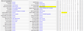
I'm seeing unexpected behavior: when I plug in USB-C only (VAC2 = 20V confirmed), Q2 does not turn on and the system (SYS) remains unpowered. ACDRV2 stays low and REGN is also 0V. I have verified the following:

  • TS pin is connected via a divider to REGN and GND (R35 = 10kΩ, R36 = 4.7kΩ), which normally yields ~1.9V when REGN is up.

  • VAC2 = 20V from TPS25751 (confirmed)

  • VAC1 is floating (nothing plugged into PLUG)

  • Q2 is a back-to-back CSD87501L controlled by ACDRV2

My understanding is that REGN should come up when BQ25798 detects a valid input and TS voltage. But it seems we’re in a cold-start deadlock:

  • REGN is off → TS = 0V → ACDRV2 is off → Q2 is off → no power reaches SYS → REGN stays off.

I've attached the relevant schematic for your reference.

Thanks in advance for your help!

output3.pdf

  • Hi  Don,

    Do you have a battery attached?  If so, what do the status, fault and voltage ADC registers report?  If you toggle the DISACDRVx bit in REG0x12[7], does that help? 

    If no battery is attached, I suspect the charger auto sets EN_HIZ bit=1 due to SYS falling below VSYS_SHORT = 2V during the attempted switchover. 

    BTW, TS fault does not prevent converter power up including REGN coming up, only charge current flowing from SYS to BAT.

    Regards,

    Jeff  

  • Hi Jeff,

    Yes, I do have a 4-cell (4S) Li-ion battery pack connected to BAT, and TPS25751 is negotiating 20V via USB-C and supplying PPHV. The TS pin is biased to ~1.73 V via resistor divider, and REGN is up at 5.03 V.

    Here’s what I observe with the battery attached:

    • Fault Status (REG0x0E): 0xA23D
      → Still includes VBUS_UVLO, VBUS_OVP, VAC_OVP, VAC_UVLO, IBUS_OCP, and VBAT_OVP

    • ADC Status (REG0x0B): 0xEA00
      → Indicates ADC is done, but no valid conversion appears

    • VBUS/VBAT/VSYS/TS ADCs: All return 0x0000

    • REG0x12 Before Toggle: 0x8100

    • After clearing DIS_ACDRV1 (bit 7): 0x0100, but the value reverts or has no effect — faults persist

    To help debug, I hardwired PPHV (TPS25751 20V output) directly to the VBUS pin (TP3 to TP4), confirming 20.59 V is present at the test point. However, it seems VBUS is still not being internally sensed. Continuity from TP4 to the actual VBUS pin on the IC is now being verified.

    Also, VAC is floating in this design, which might explain persistent VAC_OVP/UVLO faults. I plan to temporarily tie VAC to PPHV or GND to rule this out.

    Let me know if there's any additional register or waveform you'd recommend probing. Appreciate the insight on EN_HIZ and TS handling — I was under the impression TS_HOT blocked converter startup, but good to know REGN and SYS can still power.

    Best regards,

    Don

  • Here is a dump of all the registers:   I am not sure if this is any help.   

    My current setup:

    Power Source:  USB-C.  {TP4 is jumped with a wire to TP3 to enable USB-C}
    No External Power,  Battery Pack connected.  4 cell 18650 with combine voltage of 15.3V

    REG 0x00: 0x0626
    REG 0x01: 0x9006
    REG 0x02: 0x0090
    REG 0x03: 0xC800
    REG 0x04: 0xBEC8
    REG 0x05: 0x01BE
    REG 0x06: 0x2C01
    REG 0x07: 0xCA2C
    REG 0x08: 0x0ACA
    REG 0x09: 0xE30A
    REG 0x0A: 0x00E3
    REG 0x0B: 0xEA00
    REG 0x0C: 0x17EA
    REG 0x0D: 0x3D17
    REG 0x0E: 0xA23D
    REG 0x0F: 0x00A2
    REG 0x10: 0x0000
    REG 0x11: 0x0000
    REG 0x12: 0x8100
    REG 0x13: 0x9C81
    REG 0x14: 0xAA9C
    REG 0x15: 0xC0AA
    REG 0x16: 0x7AC0
    REG 0x17: 0x547A
    REG 0x18: 0x0154
    REG 0x19: 0x2C01
    REG 0x1A: 0x0D2C
    REG 0x1B: 0x100D
    REG 0x1C: 0x0110
    REG 0x1D: 0xC001
    REG 0x1E: 0x01C0
    REG 0x1F: 0x0001
    REG 0x20: 0x0000
    REG 0x21: 0xFD00
    REG 0x22: 0x1200
    REG 0x23: 0x1000
    REG 0x24: 0x1100
    REG 0x25: 0x2000
    REG 0x26: 0x0000
    REG 0x27: 0x0000
    REG 0x28: 0x0000
    REG 0x29: 0x0000
    REG 0x2A: 0x0000
    REG 0x2B: 0x0000
    REG 0x2C: 0x0000
    REG 0x2D: 0x3000
    REG 0x2E: 0x0030
    REG 0x2F: 0x0000
    REG 0x30: 0x0000
    REG 0x31: 0x0000
    REG 0x32: 0x0000
    REG 0x33: 0x0000
    REG 0x34: 0x1F86
    REG 0x35: 0x861F
    REG 0x36: 0x0000
    REG 0x37: 0x0000
    REG 0x38: 0x0000
    REG 0x39: 0x0000
    REG 0x3A: 0x0000
    REG 0x3B: 0x0000
    REG 0x3C: 0x0000
    REG 0x3D: 0x0000
    REG 0x3E: 0x0000
    REG 0x3F: 0x0000

  • HI Don,

    The VACx pins cannot be left floating.  They either need to be tied to VBUS if no MUX FETS are used and ACDRVx=GND or connected to the input side of the of corresponding MUX FETS.  

    Regards,

    Jeff

  • Hi Jeff,

    Thanks for the clarification.

    In my design, I am using two external ACFETs (CSD87501L), controlled by ACDRV1 and ACDRV2. The VAC1 and VAC2 pins are each connected to the source of their respective FETs:

    • VAC1 is tied to the PLUG input (source of Q1) -  External Power Source

    • VAC2 is tied to the USB-C PPHV input (source of Q2 from TPS25751) - USB-C power source

    So the VACx pins are not floating and are correctly routed to the input side of the external NFETs, as per your guidance.

    Currently, I’ve temporarily added a 10k pull-up from ACDRV2 to TP4 (PPHV) to test the FET behavior manually. I am reading ~5.6V on ACDRV2 — it's externally pulled up, not driven by the charger.   I am not sure if the FET is bad, or I have a bad design (probably the latter).   

    I am still tripping all the faults and the ADC are not detecting any voltage.   

    Fault Status (0x0E) = 0xA63D1010 0110 0011 1101

    Reading ADCs...

    ADC Status (0x0B): 0xEA00
    Fault Status (0x0E): 0xA63D
    VBUS ADC (0x27): 0x0000 → 0 mV
    VBAT ADC (0x28): 0x0000 → 0 mV
    VSYS ADC (0x2A): 0x0000 → 0 mV
    TS ADC (0x2C): 0x0000 → 0 mV
    Input Source Control (REG0x0A): 0x000B
    IINDPM (REG0x06): 0x2C01
    ACDRV Control (REG0x12): 0x8100

    Can you suggest any possible temporary fix to try to get the system working.   I can do a respin, but need to get the basic working first.  

    Best regards,
    Don

  • Hi Don,

    I am puzzled by your reads.   Each register is 8 bits but you have more than that shown.

    Regards,

    Jeff

  • Jeff,

    Very sorry about that.  The code was written by Chat-GPT.   Here is the updated register dump:   This is with the external plug power running and the batteries connected.  Not sure why TS_HOT_FAULT is tripped.  The TS voltage is 1.7.   

    📋 BQ25798 Register Diagnostic
    
    🔹 8-bit Registers:
      REG 0x00: 0x04
      REG 0x08: 0xCA
      REG 0x09: 0x0A
      REG 0x0A: 0x0B
      REG 0x15: 0xAA
      REG 0x1A: 0x0C
      REG 0x1E: 0xC0
      REG 0x1F: 0x01
      REG 0x20: 0x20
      REG 0x21: 0x00
      REG 0x22: 0x00
      REG 0x30: 0x00
      REG 0x31: 0x00
      REG 0x32: 0x00
      REG 0x33: 0x00
      REG 0x3E: 0x00
      REG 0x3F: 0x00
    
    🔹 16-bit Registers:
      REG 0x01: 0xA401
      REG 0x03: 0x6400
      REG 0x05: 0x00AE
      REG 0x07: 0xCA0C
      REG 0x0B: 0xEA00
      REG 0x0D: 0x3D17
      REG 0x0E: 0x823D
       ⚠️  Fault Bits:
         - OTG_OVP
         - IBUS_OCP
         - VAC1_UVLO
         - VAC2_UVLO
         - VBUS_UVLO
         - VBUS_OVP
         - TS_HOT_FAULT
      REG 0x1B: 0x100B
       🟢 Charger/System Status:
         - Watchdog Fault: ❌
         - IBUS DPM Active: ❌
         - VINDPM Active: ❌
         - IIN_LIMIT Low: ✅
         - Power Good (PG): ✅
         - VBUS Present: ✅
      REG 0x1C: 0x0110
       🔋 Charge State:
         - Charge State: Not Charging
         - VSYS Ready: False
         - Battery Present: False
         - Input Valid: False
      REG 0x23: 0x0000
      REG 0x25: 0x2000
      REG 0x27: 0x0000
      REG 0x28: 0x0000
      REG 0x2A: 0x0000
      REG 0x2C: 0x0000
      REG 0x2E: 0x0030
      REG 0x34: 0x4900
      REG 0x36: 0x0061
    

  • Hi Don,

    TS_HOT is disabling charge.  Is there a thermistor or 10k ohm resistor from TS to ground to simulate a thermistor?

    Regards,

    Jeff

  • Hi Jeff,

    I have a resistor divider network (modified from uploaded schematic),   The current board is 

    REGN (Measured: 5.02 V )
    |
    [R40 = 100k]
    |
    TS pin  (Measured: 1.72 V)
    |
    [R44 = 52.5k]
    |
    AGND

    My understanding is that the Normal TS should be in the range of 0.8V and 2.4V and I am at 1.72V.   So I don't fully understand why TS is whacked out.    I have tried performing a reset of the BQ by writing 0x80 to register 0x32.   But that does seem to effect the TS.   (My reset routine is below).   Do you see any issues on the schematic that might cause these issues?   

    My reset routine is the following:

    from smbus2 import SMBus
    import time
    
    I2C_BUS = 1
    BQ25798_ADDR = 0x6B
    
    def read_register(bus, addr, reg, length=2):
        data = bus.read_i2c_block_data(addr, reg, length)
        return int.from_bytes(data, byteorder='little')
    
    def write_register(bus, addr, reg, value, length=2):
        data = value.to_bytes(length, byteorder='little')
        bus.write_i2c_block_data(addr, reg, list(data))
    
    def main():
        with SMBus(I2C_BUS) as bus:
            print("🔧 Resetting BQ25798...")
    
            # Step 1: Trigger soft reset
            print(" → Sending RESET (REG 0x32 = 0x80)")
            write_register(bus, BQ25798_ADDR, 0x32, 0x80)
            time.sleep(0.2)  # Allow reset to complete
    
            # Step 2: Reconfigure recommended post-reset defaults
            print(" → Configuring input thresholds (REG 0x0A = 0x000B)")
            write_register(bus, BQ25798_ADDR, 0x0A, 0x000B)
    
            print(" → Setting IINDPM = 3A (REG 0x06 = 0x0C00)")
            write_register(bus, BQ25798_ADDR, 0x06, 0x0C00)
    
            print(" → Enabling ADC channels (REG 0x32 = 0x00FF)")
            write_register(bus, BQ25798_ADDR, 0x32, 0x00FF)
    
            print(" → Starting ADC conversion (REG 0x33 = 0x8000)")
            write_register(bus, BQ25798_ADDR, 0x33, 0x8000)
    
            # Clear DIS_ACDRV2 (bit 7) in REG0x12
            reg_12 = read_register(bus, BQ25798_ADDR, 0x12)
            reg_12 &= ~(1 << 7)  # Clear bit 7
            write_register(bus, BQ25798_ADDR, 0x12, reg_12)
            print(f"Updated REG0x12: 0x{reg_12:04X}")
    
            print("✅ Reset and reconfiguration complete.\n")
    
    if __name__ == "__main__":
        main()
    

  • Hi Don,

    When V(TS) drops to 34% of REGN, the charger is in TS HOT.

    You can hardware disable TS by sizing the resistor divider to set V(TS) = 2.5V=50%*REGN or use the IGNORE_TS bit REG0x18[0].

    Regards,

    Jeff

  • Jeff,

    Thank you for the updated information.   Something I missed.   I have updated the resistor values that TS = 2.73V.   But 0x2C is reading 0mV.   And TS_FAULT is still active.    I have tried to set IGNORE_TS=1 (sudo i2cset -y 1 0x6B 0x18 0x5500 w), but I think the watchdog timer is resetting it.  It sticks around for a few seconds then it reverts.   

    What works - Appears that the PLUG power works and charges the battery, but I am limited to 1 Amp, probably because of fault.   My ILIM_HIZ is set to provide maximum power.   

    What still not working:  USB-C is not kicking on.    I am not sure what to do next.

    Register Dump 

    Address    | Name                             | Value      | Meaning
    --------------------------------------------------------------------------------
    0x00       | Minimum System Voltage           | 0x26       | 
    0x01       | Charge Voltage Limit             | 0x9006     | 
    0x03       | Charge Current Limit             | 0x6400     | 
    0x05       | Input Voltage/Current Limit      | 0x00B0     | 
    0x07       | Charge Option 0                  | 0xC382     | 
    0x08       | Pre-Charge/Termination Current   | 0xC3       | 
    0x09       | Charge Voltage Top-Off Timer     | 0x05       | 
    0x0A       | Input Source Control             | 0xE3       | 
    0x0B       | ADC Status                       | 0xDC00     | 
    0x0D       | Fault Status 1                   | 0x3D4B     | 
    0x0E       | Fault Status 2                   | 0xA23D     | OTG_OVP, VBAT_OVP, IBUS_OCP, VAC1_UVLO, VAC2_UVLO, VBUS_UVLO, VBUS_OVP, TS_FAULT
    0x12       | ACDRV Control                    | 0x4100     | ACDRV1 (PLUG): ON, ACDRV2 (USB-C): ON
    0x15       | Converter Control 0              | 0xAA       | 
    0x18       | Charger Control 3                | 0x54       | IGNORE_TS=No, BATFET_CTRL=Off
    0x1A       | Charge Option 1                  | 0x82       | 
    0x1B       | Charger Status 1                 | 0x6AAB     | PG=Yes, VBUS=Yes
    0x1C       | Charger Status 2                 | 0x016A     | State=Charge Termination, VSYS_RDY=False, BAT=True, IN_OK=False
    0x1E       | JEITA IIN                        | 0x40       | 
    0x1F       | JEITA VSYS                       | 0x00       | 
    0x20       | PROCHOT Status Mask              | 0x00       | 
    0x21       | PROCHOT Control                  | 0x00       | 
    0x22       | ILIM/VINDPM Control              | 0x00       | EXT_ILIM=Disabled, EXT_VINDPM=Disabled
    0x23       | VAC1 ADC                         | 0x0000     | 
    0x25       | VAC2 ADC                         | 0x0000     | 
    0x27       | VBUS ADC                         | 0x0000     | 0 mV
    0x28       | VBAT ADC                         | 0x0000     | 0 mV
    0x2A       | VSYS ADC                         | 0x0000     | 0 mV
    0x2C       | TS ADC                           | 0x0000     | 0 mV (TS)
    0x2E       | IIN ADC                          | 0x0030     | 48 mA (Input Current)
    0x30       | ADC Control                      | 0x00       | 
    0x31       | Function Control 0               | 0x00       | 
    0x32       | ADC Channel Enable               | 0x00       | 
    0x33       | ADC Conversion Start             | 0x00       | 
    0x34       | IBAT ADC                         | 0x4A00     | 
    0x36       | VOUT ADC                         | 0x006D     | 
    0x3E       | Reserved                         | 0x00       | 
    0x3F       | Reserved                         | 0x00       | 
    

  • Hi Don,

    Yes, watchdog resets Ignore TS.  So you might want to disable watchdog timer.

    I'm still struggling to read your data from the registers as some are reading 4 numbers but shouldn't be. The status and fault registers from 0x1B to 0x27 are the most important for debug.  Reduced charge current can be from:

    CV/Taper - V(BATP)=VREG

    IINDPM - input current limit 

    VINDPM - if you register reading above is correct, it is set to 17.6V.  VINDPM cannot be disabled but the threshold can be lowered.

    TREG - die temp is too hot - likely not your issue.

    Regarding the PD controller, I will have to involve someone from the PD team.

    Regards,

    Jeff

  • Jeff,

    Apologies for the earlier confusion in the register dumps. I've been using ChatGPT to help generate Python code to extract data from the BQ25798 registers — it’s admittedly quicker than having an old hardware engineer write it all by hand.

    I've now reworked the script to align with your specific request and believe I’ve captured all the relevant registers you outlined (0x1B through 0x27), along with a few others related to input current, VINDPM, and VBAT. The output now includes both raw and interpreted values for clarity.

    Current configuration:

    • External supply: 18.95 V connected to PLUG

    • USB-C PD source: 20 V connected to PPHV

    • 4-cell battery connected

    • System load: ~600 mA

    Let me know if you'd like additional registers or a different format. I really appreciate your support in working through this.


     BQ25798 Diagnostic Snapshot

    Reg Name Raw Value Meaning
    0x06 IINDPM (Input Current Limit) 0x8200 (LSB=0x00, MSB=0x82) 512 mA (IINDPM)
    0x0A Input Source Control (VINDPM) 0xE3 VINDPM = 25.9 V
    0x0E Fault Status 2 0xA23D (LSB=0x3D, MSB=0xA2) TREG Fault = No
    0x22 ILIM/VINDPM Control 0x80 EXT_ILIM = Disabled, EXT_VINDPM = Disabled
    0x28 VBAT ADC 0x0000 (LSB=0x00, MSB=0x00) VBAT = 0 mV

     BQ25798 Debug Registers (0x1B–0x27)

    Reg Name Raw Value Meaning
    0x1B Charger Status 1 0x6AAB (LSB=0xAB, MSB=0x6A) PG = Yes, VBUS = Yes
    0x1C Charger Status 2 0x016A (LSB=0x6A, MSB=0x01) Charge State = Termination, VSYS_RDY = False, BAT = True, IN_OK = False
    0x22 ILIM/VINDPM Control 0x80 EXT_ILIM = Disabled, EXT_VINDPM = Disabled
    0x23 VAC1 ADC 0x0080 (LSB=0x80, MSB=0x00) 2048 mV
    0x25 VAC2 ADC 0x0000 (LSB=0x00, MSB=0x00) 0 mV
    0x27 VBUS ADC 0x0000 (LSB=0x00, MSB=0x00) 0 mV

    Let me know what stands out or if you'd like me to test anything further.

    Best regards,
    Don

  • HI Don,

    REG0x1B - 0x27 are only 8 bit registers so those values above don't make sense to me.  Below is snapshot from BQSTUDIO software:

    If you can separate out the values, I can tell you which state/fault is limiting the current.

    Regards,

    Jeff

  • Hi Jeff,

    Chalk this up to one of the current limitations of AI — even after being corrected once, it doesn’t consistently remember which registers are 8-bit vs 16-bit. I’ve since rebuilt the script to properly handle register widths based on the datasheet, so everything shown below reflects accurate reads.

    I’d love to use BQStudio, but my environment is purely Linux. I’m using a Raspberry Pi connected over I²C and pulling data via Python scripts.

    Here’s the output from the latest run:


     BQ25798 Diagnostic Snapshot (16-bit Registers)
    (Read via correct word-length for each register)

    Reg Name Raw Value Meaning
    0x06 IINDPM (Input Current Limit) 0x8200 (LSB=0x00, MSB=0x82) 512 mA (IINDPM)
    0x0E Fault Status 2 0xA23D (LSB=0x3D, MSB=0xA2) TREG Fault = No
    0x28 VBAT ADC 0x0000 (LSB=0x00, MSB=0x00) VBAT = 0 mV

     Debug Registers 0x1B–0x27 (8-bit Registers)
    (Read individually as bytes, as expected in BQStudio)

    Reg Name Raw Value Meaning
    0x0A Input Source Control (VINDPM) 0xE3 VINDPM = 25.9 V
    0x1B Charger Status 1 0x2B PG = Yes, VBUS = Yes
    0x1C Charger Status 2 0xEA State = Unknown, VSYS_RDY = False, BAT = True, IN_OK = False
    0x22 ILIM/VINDPM Control 0x00 EXT_ILIM = Disabled, EXT_VINDPM = Disabled
    0x23 VAC1 ADC 0x00 0 mV
    0x25 VAC2 ADC 0x00 0 mV
    0x27 VBUS ADC 0x00 0 mV

    Let me know if anything stands out or if you’d like me to collect anything else.

    Best,
    Don

  • Hi Don,

    We are getting closer.  

    REG0x06 cannot be 0.x82.

    REG0x0E is not 4 numbers.

    Status 0x1B and 0x1C are reporting charge termination done.

    Is that true?

    Regards,

    Jeff

  • Hi Jeff,

    Thanks again for sticking with me. I've corrected the register handling (I believe):

    - REG 0x06 is now properly masked to 12 bits (IINDPM)
    - REG 0x0E is interpreted as fault bits (not raw value formatting)

    The first snapshot was taken with:
    - 600 mA load
    - PLUG (18.6 V) active
    - USB-C present but not sourcing power
    - Battery was fully charged; this captures re-entry into charge phase

    BQ25798 Diagnostic Snapshot – PLUG Active

    Reg | Name | Raw Value | Meaning
    -------|------------------------------|--------------------------------|-------------------------------
    0x06 | IINDPM | 0x8200 (LSB=00, MSB=82) | 512 mA (masked to 12 bits)
    0x0E | Fault Status 2 | 0xA23D (LSB=3D, MSB=A2) | TREG Fault = No (others active)
    0x28 | VBAT ADC | 0x0000 | VBAT = 0 mV

    Reg | Name | Raw Value | Meaning
    -------|------------------------------|------------|----------------------------------------------
    0x0A | Input Source Control | 0xE3 | VINDPM = 25.9 V (likely too high)
    0x1B | Charger Status 1 | 0xAB | PG = Yes, VBUS = Yes
    0x1C | Charger Status 2 | 0x6A | Charge = Termination, BAT = True, IN_OK = False
    0x22 | ILIM/VINDPM Control | 0x00 | EXT_ILIM = Disabled, EXT_VINDPM = Disabled
    0x23 | VAC1 ADC | 0x00 | 0 mV
    0x25 | VAC2 ADC | 0x00 | 0 mV
    0x27 | VBUS ADC | 0x00 | 0 mV

    VBAT still reads 0 mV despite BAT being reported as present — I suspect either a TS latch or a power path condition blocking charge current. Lowering VINDPM is my next step.

    ---

    This second snapshot is with PLUG disconnected, USB-C connected (20 V), and the same 600 mA load.

     BQ25798 Diagnostic Snapshot – USB-C Only

    Reg | Name | Raw Value | Meaning
    -------|------------------------------|--------------------------------|-------------------------------
    0x06 | IINDPM | 0x8200 (LSB=00, MSB=82) | 512 mA
    0x0E | Fault Status 2 | 0xA23D (LSB=3D, MSB=A2) | TREG Fault = No
    0x28 | VBAT ADC | 0x0000 | VBAT = 0 mV

    Reg | Name | Raw Value | Meaning
    -------|------------------------------|------------|----------------------------------------------
    0x0A | Input Source Control | 0xE3 | VINDPM = 25.9 V
    0x1B | Charger Status 1 | 0x20 | PG = No, VBUS = No
    0x1C | Charger Status 2 | 0x00 | Not Charging, BAT = False, IN_OK = False
    0x22 | ILIM/VINDPM Control | 0x5B | EXT_ILIM = Disabled, EXT_VINDPM = Enabled
    0x23 | VAC1 ADC | 0x90 | 4096 mV
    0x25 | VAC2 ADC | 0x00 | 0 mV
    0x27 | VBUS ADC | 0x00 | 0 mV

    It seems USB-C is not being accepted as a valid source — VBUS and IN_OK remain low. Let me know if you’d recommend debugging that path next.

    Best regards,
    Don

  • Jeff,

    I just ordered the EV2400, will be in Thursday.   I will get the BQStudio up and running to help with the debugging.  Do I need anything else?   I am assuming my attempt python code has fallen flat.     Also, did you get a chance to look at the schematic to see if there anything else.    One of my colleagues suggested that instead of using dual VAC1/2 inputs,  drop VAC2 and use a OR'ing IC (LM74700-Q1) to switch everything to VAC1 since that is working.     What do you think of this suggestion?   

    Don

  • Hi Don,

    BQ2400 +BQSTUDIO should make debug faster.  I haven't used an ORing IC but have used TPS2121 dual MUX with BQ25798.  The only difference in VAC1 vs VAC2 is VAC1 turn on is delayed for up to 2s in order for D+/D- detection to complete.  I wonder if the TPS25751 is unknowingly relying on that delay.

    Regards,

    Jeff

  • Jeff,

    Received my EV2400 in today and got BQStudio up and running.   Lots and lots of data..  What test / collections do you now need?   Attached is register dump and screen shot with the battery plugged in, usb-c connected and plug power on.

    * Created: Thu Jun 26 16:36:41 EDT 2025
    *
    * Format: Register Name  tab Character,\t  Register Address  tab Character,\t  Hexadecimal register value.
    * Device: BQ25798
    * BQZ Container: Charger_1_01-BQ25798.bqz
    *
    REG00	26
    REG01	0000
    REG03	0064
    REG05	24
    REG06	012C
    REG08	C3
    REG09	05
    REG0A	E3
    REG0B	00DC
    REG0D	4B
    REG0E	3D
    REG0F	A6
    REG10	85
    REG11	40
    REG12	00
    REG13	41
    REG14	1E
    REG15	AA
    REG16	C0
    REG17	7A
    REG18	54
    REG19	0032
    REG1B	2F
    REG1C	0A
    REG1D	00
    REG1E	40
    REG1F	10
    REG20	00
    REG21	00
    REG22	2F
    REG23	12
    REG24	40
    REG25	10
    REG26	00
    REG27	00
    REG28	00
    REG29	00
    REG2A	00
    REG2B	00
    REG2C	00
    REG2D	00
    REG2E	30
    REG2F	00
    REG30	00
    REG31	0000
    REG33	0000
    REG35	0000
    REG37	0000
    REG37	0000
    REG3B	0000
    REG3D	0000
    REG3F	0000
    REG41	0000
    REG43	0000
    REG45	0000
    REG47	00
    REG48	19
    Screen Shot

  • Hi Don,

    Congrats on getting the EV2400 and BQSTUDIO up and running! EN_HIZ bit =1 which means the converter is off.  The charger only auto sets that bit in the event of a either low voltage on SYS after power up (it thinks there is a short) or inductor current > cycle current limit which is 7.5A or poor source detection at power up.  The fault flag reports VSYS short or CONVTER OCP or POOR SRC respectively.  Did the fault flags report either event?  Those flags clear after being read.

    Also, watchdog timer has expired so changes to several registers will revert back to defaults.  Until we finish debug you might want to disable watchdog timer.

    Regards,

    Jeff

  • Hi Jeff,

    Thanks for the insights. We're still in the process of isolating a possible short by removing subsystems one at a time.

    We’ve observed that even after setting 0x00 to output 16.8V on SYS, the BQ25798 reverts to 12V on each power cycle. We're currently programming the TPS25751 EEPROM using 16.8V input, so we’re wondering:
    – Is this behavior expected from the TPS25751 reapplying register settings at startup, or is the BQ defaulting due to a fault condition?

    Regarding your questions:

    • We have not yet confirmed the specific fault flags—we’ll rerun a capture while checking VSYS_SHORT, CONV_OCP, and POORSRC bits before they clear.   Is there a way to export from BQStudio to provide you a clean export?  

    • We’ll also disable the watchdog timer as suggested to ensure our register settings persist during debugging.

    Thanks again for the guidance.

    Best,
    Don

  • HI Don,

    The charger reverts to defaults per PROG pin resistor after POR (both VBUS and VBAT) or WD timer expiration:

    I'm not exactly certain what the TPS25751 writes for MINSYS but I suspect it is close the values above.

    Regards,

    Jeff

  • Good news first: after fixing the 12 V buck I was able to power the system from USB-C and charge the battery at 1 A by tweaking a few BQStudio registers. Unfortunately, every reboot forces the charger back into fail-safe mode and I haven't been able to get back into charging mode. The board is running from USB-C, but the battery no longer charges and the registers reset to their defaults.

    • Reg 0x1C reads “Not charging” and “VBUS: non-qualifying adapter.” I’m using Apple’s 100 W USB-C power brick, which should qualify.

    A register dump taken immediately after boot is attached.

    Could you help me understand:

    1. Why this adapter is being marked non-qualifying, and

    2. How to clear fail-safe mode so normal charging survives a reboot?

    We’re very close, but I’m missing the last piece of the puzzle.

    Thanks for your guidance.

    * Created: Mon Jun 30 16:06:54 EDT 2025
    *
    * Format: Register Name  tab Character,\t  Register Address  tab Character,\t  Hexadecimal register value.
    * BQZ Container: Charger_1_01-BQ25798.bqz
    *
    REG00	00	36
    REG01	01	690
    REG03	03	12C
    REG05	05	BE
    REG06	06	12C
    REG08	08	CA
    REG09	09	0A
    REG0A	0A	E3
    REG0B	0B	EA
    REG0D	0D	17
    REG0E	0E	3D
    REG0F	0F	A2
    REG10	10	00
    REG11	11	00
    REG12	12	00
    REG13	13	81
    REG14	14	9C
    REG15	15	AA
    REG16	16	C0
    REG17	17	7A
    REG18	18	55
    REG19	19	12C
    REG1B	1B	0D
    REG1C	1C	90
    REG1D	1D	01
    REG1E	1E	C0
    REG1F	1F	00
    REG20	20	00
    REG21	21	00
    REG22	22	00
    REG23	23	00
    REG24	24	00
    REG25	25	00
    REG26	26	00
    REG27	27	00
    REG28	28	20
    REG29	29	80
    REG2A	2A	00
    REG2B	2B	00
    REG2C	2C	00
    REG2D	2D	00
    REG2E	2E	30
    REG2F	2F	00
    REG30	30	00
    REG31	31	00
    REG33	33	00
    REG35	35	1DE5
    REG37	37	00
    REG37	39	00
    REG3B	3B	00
    REG3D	3D	00
    REG3F	3F	00
    REG41	41	00
    REG43	43	00
    REG45	45	00
    REG47	47	00
    REG48	48	19

  • Jeff,

    It looks like the BQ25798 is fundamentally working, but it consistently drops into fail-safe mode on every power-up. I can re-enable charging in BQStudio and the pack charges at 1 A, but after the next power cycle it’s back in fail-safe.

    Could this behavior point to a schematic or layout issue on our end?

    Key facts:

    • TPS25751 successfully negotiates 20 V sink and drives PPHV.
    • 4-cell pack (16.8 V) present on BAT; NTC reads valid.
    • All three power paths (USB-C, PLUG, battery) can boot the load at 12V, so the OR-ing path is intact.
    • Watchdog is still at its 30 s default; any register changes revert unless I keep the bus active.  I don't think I can permanently disable it or haven't been able to do so yet.  

    • Attached is the current register dump taken right after re-enabling charging.

    Questions:

    1. Which specific fault(s) would force the device into fail-safe even though voltage and current limits appear within spec?

    2. Could any of our component choices (divider values, ILIM resistor, TS network, etc.) or the VAC1/VAC2 routing contribute to this?

    3. Is there a recommended POR sequence or watchdog setting that avoids this corner case?

    Appreciate any guidance—let me know if another set of scope shots or the schematic would help.

    Thanks,

    Don

    * Created: Tue Jul 01 09:34:21 EDT 2025
    *
    * Format: Register Name  tab Character,\t  Register Address  tab Character,\t  Hexadecimal register value.
    * BQZ Container: Charger_1_01-BQ25798.bqz
    *
    REG00	00	36
    REG01	01	690
    REG03	03	12C
    REG05	05	BE
    REG06	06	12C
    REG08	08	CA
    REG09	09	0A
    REG0A	0A	E3
    REG0B	0B	EA
    REG0D	0D	17
    REG0E	0E	3D
    REG0F	0F	A2
    REG10	10	00
    REG11	11	00
    REG12	12	00
    REG13	13	41
    REG14	14	1C
    REG15	15	AA
    REG16	16	C0
    REG17	17	7A
    REG18	18	55
    REG19	19	12C
    REG1B	1B	0F
    REG1C	1C	90
    REG1D	1D	01
    REG1E	1E	C0
    REG1F	1F	00
    REG20	20	00
    REG21	21	00
    REG22	22	00
    REG23	23	00
    REG24	24	00
    REG25	25	00
    REG26	26	00
    REG27	27	00
    REG28	28	20
    REG29	29	80
    REG2A	2A	00
    REG2B	2B	00
    REG2C	2C	00
    REG2D	2D	00
    REG2E	2E	B0
    REG2F	2F	00
    REG30	30	00
    REG31	31	53E
    REG33	33	36F
    REG35	35	4C26
    REG37	37	4C36
    REG37	39	50DE
    REG3B	3B	4168
    REG3D	3D	41CC
    REG3F	3F	157
    REG41	41	6E
    REG43	43	229
    REG45	45	29F
    REG47	47	00
    REG48	48	19

  • Hi Don,

    The WD timer can be disabled by writing REG0x10[2:0]=000.  The charge status register is reporting taper charger (constant voltage mode) meaning the battery voltage sensed at BATP =VREG.  As the battery pack cells charge, ICHG = (VREG-VCELLS) / Resistance where resistance is the sum of the trace, cable, connector, pack protector resistances. 

    Regarding 1, there are no faults that reset registers to default.  Registers only get reset to default if both VBUS and VBAT fall below their respective UVLO thresholds OR by writing REG0x09[6]=1.

    Regarding 2, for your registers attached, no.  The charger is working as expected. VACx is a high impedance input pin that senses input voltage.  As long as there is a 0.1uF filter cap near the IC, I do not expect VACx to cause an issue.

    Regarding 3, if the processor could be shut down at some point and not provide the WD ping, I recommend disabling watchdog timer.  Then, after the USB-C contract is complete, the ICHG, VREG, IINDPM, VINDPM and EN_LIM register bits should be written.

    Regards,

    Jeff

  • Hi Jeff,

    Great news—USB-C input, external adapter input, and battery charging now all work after power-on. A couple of points still need clarification:

    1. SYS-node capacitance
      I originally had ~100 µF of X7R ceramics on SYS. On cold boot the charger pulled ~0.5 A and often fell into fault. After halving the bulk to ~50 µF it starts and charges reliably. Is there a recommended maximum effective capacitance for SYS, or a guideline for inrush that I should follow?

    2. VSYSMIN POR default
      Register 0x00 always reverts to 12 V at POR. Can the device retain a 16 V VSYSMIN across resets, or will I need to redesign the 12 V buck/boost stage to accommodate the 12 V default?

    Thanks for your help.

  • Hi Don, sorry for the delay. Jeff is currently on time bank and will get back to you on Thursday.

  • HI Don,

    Regarding 1, that is odd.  I have other customers with that much capacitance or more at SYS.  I will confirm with designer.  When you say "feel into fault", what happens exactly?  IC damaged?  

    Regarding 2, SYSMIN default resets to default per PROG pin after both VBUS and VBAT fall below their respective UVLOs.  Unfortunately that can't be changed.

    Regards,

    Jeff