This thread has been locked.

If you have a related question, please click the "Ask a related question" button in the top right corner. The newly created question will be automatically linked to this question.

TPS92692-Q1: Before VCC UV, the gain of CSP-CSN <<14

Part Number: TPS92692-Q1

Tool/software:

Hi team,

Could you please share your suggestions for the following question? Thanks!

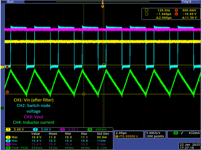
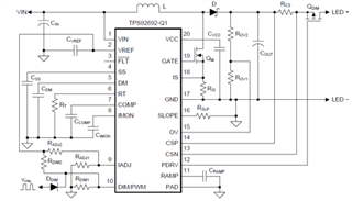
Key parameters: RCS=1.8Ω | | 1.5Ω=0.82Ω,V_IADJ=5V.

Therefore, the theoretical value of Iout is: Iout=V_IADJ_Clamp/Gain/Rcs=2.4V/14/0.82Ω=209mA.

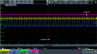
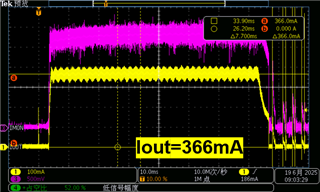
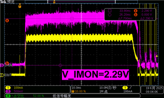
Test 1: IOUT=366mA, VIMON=2.29V when Vin=5.2V, near UV, this triggers the overcurrent protection of the IS pin.

Based on the test results, reverse GAIN by the formula, Gain=V_IADJ_Calmp/(Iout*Rcs)=2.29V/(366mA*0.82Ω)=7.63<<14.

Test 2: When Vin=13.5V, Iout=200mA or so, Gain ≈ 14 is displayed and normal is restored.

Please help analyze why the Gain of CSP-CSN is getting lower before UV. Thanks!

Regards,

Ivy

  • Ivy, 

    Please provide the following information:

    Schematic and PCB layout.

    Input/ output requirements and switching frequency:

    Inductor current
    Switch node voltage
    Input voltage
    Output voltage


    This is what your scope shot should look like, the channels are labeled in the picture and I need the same time division:


    Best,
    Daniel Louis

  • Hi Daniel,

    Please see the attachment. Thanks.

    TPS92692-Q1 issue.pptx

    Regards,

    Ivy

  • Hi Iyv, 

    Thank you so much for all the information. It was really informative and provided us with clarity to diagnose this issue. 

    I know the data sheet for this part lists Vin_min as 4.5V, but you really need to be above the LDO, VCC, and VDD voltages. In the event you wish to lower Vin below 7.5V, you have to power VCC and VDD with a separate power supply. 

    Please see the block diagram for more information.


    Best,
    Daniel

  • Hi Daniel,

    Thanks for your comments!

    1. Currently, it is difficult for customer to introduce another separate power supply to power VCC and VDD.  The low voltage input test for the 6V Vin is a requirement from the CAR OEM, as there is a potential 300ms VIN low voltage risk at the ignition moment. 

    May I ask whether there are other ways to optimize this problem?

    2. Could you help share why the low Vin affects the value of GAIN from the principle perspective? 

    Regards,

    Ivy

  • Hi Ivy, 

    1. Unfortunately there is no way past this other than what I mentioned above. The converter cannot operate properly if VCC and VDD are not getting the voltage they need.

    2. The low Vin doesn't directly effect the gain, as the gain is fixed. The real issue here is that the converter is unable to operate properly at such a low Vin.

    Best,
    Daniel

  • Hi Daniel,

    Understood, thanks for your comments.

    Based on your experience, how do other customers solve this problem? This is because many car OEMs now require low VIN start tests, as shown in the following figures. 

    If they add a DCDC to the front stage for voltage regulation, the cost is relatively high. 

    Regards,

    Ivy

  • Hi Ivy, 

    I think I misdiagnosed this issue and I will investigate it more deeply today. I sincerely apologize. You can definitely run this device at 6V, you will simply need to use a logic-level FET and we may have to tweak a few things to get this circuit to operate properly. Again, I sincerely apologize for the mistake and I am making this a priority. 

    Best,
    Daniel

  • Hi Ivy, 

    The device is simply hitting current limit, so you really just need to lower R_IS. I set mine to 150 milliohms.

    A few things to consider:

    1. You may want to increase the input capacitance since you want to ensure stable input voltage at low line because the device will pull a lot of current. 
    2. When I initially configured the device, I noticed there was a lot of noise at Vin of the IC so I would consider added a larger capacitor at C20
    3. At low line, I saw there was a lot of noise across CSP/CSN so make sure you use a good current sense resistor and maybe look into implementing the filter in the data sheet.
      
    4. Make sure your customer adheres to the component value calculations in our calculator tool, with the exception of the considerations I mentioned above.


    CH1: Vin (~6V), CH2: VSW, CH3: ILED, CH4: VOUT

    I didnt see any visible flicker on my end. However, the converter will have an easier time operating above ~7V. so you won't witness the weird VSW wave form I pasted above at Vin_TYP.

    Please let me know how I can assist you further.

    Best,
    Daniel