Tool/software:
Hi there,
this problem is a followup of this one: https://e2e.ti.com/support/power-management-group/power-management/f/power-management-forum/1402001/bq40z80-bms-field-reject---no-access-to-memory---eeprom-erased/5414983?tisearch=e2e-sitesearch&keymatch=bq40z80%20frank#5414983
Sealing the device did not improve the situation.
We have done further testing and found that
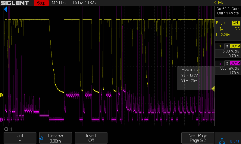
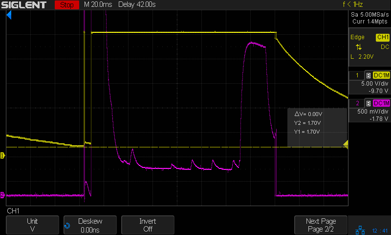
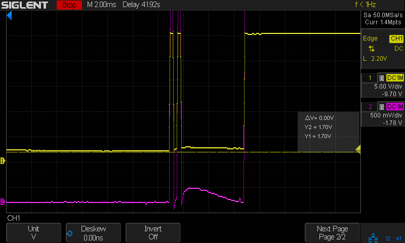
- the device stays in INIT for about 2 seconds (INIT bit of OperationStatus is set
- if we then remove power to the device (remove PACK+) it will brick itself
- when bricked, we see 0xFF in most responses from SBS commands that report flash contents (for example, 0x20 ManufacturerName)
- when bricked, it is no longer possible to unseal the device (assumption: all keys are also all 0xFF)
The device has minimal configuration as we only use it as a normal LiIon protection device with cell balancing. All the advanced features like IT, Gauging, Charging, are disabled (Mfg Status Init = 0x0010).
This application uses a removable balancing connection, that also provides GND to the chip. Because of this, and because we cannot guarantee contact bounce free insertion, we cannot ensure a stable supply voltage to the chip.
We also have failures in the field, which suggests that there might be more failure modes.
The findings above suggest that the chip makes flash writes during INIT (and maybe also during operation), which result in memory corruption and bricking the device, when power is removed at the "wrong moment".
How can we configure the device such that it will not write any data to flash during INIT and normal operation (ACTIVE, SLEEP)?
Can we get more info about what exactly it is writing in which situation?
Is it possible to mitigate this with added supply capacitance?
Is there logic in the firmware that stops flash write activity _before_ supply voltages become critical (both INIT and operation)?
Is there a flash write protection mechanism that inhibits these "background" writes?
Maybe a different firmware image that we can load onto the devices?
Any help will be greatly appreciated, as at the moment the field failure rate is significant, in the order of 5%.
Regards Frank
Here is a dump of the device configuration:
0x00, 0x00, 0x00, 0x00, 0xAC, 0x0D, 0x1E, 0x44, 0x00, 0x04, 0x20, 0x00, 0x00, 0x00, 0x00, 0x96, // 4AC0
0x00, 0xAF, 0x00, 0xE4, 0x77, 0x00, 0x00, 0x00, 0x00, 0x00, 0x00, 0x00, 0x00, 0x00, 0x00, 0x00, // 4AD0
0x00, 0x00, 0x00, 0x00, 0x00, 0x00, 0x16, 0xEA, 0x00, 0xAC, 0x0D, 0xD0, 0x07, 0x05, 0x00, 0x00, // 4AE0
0x0A, 0x00, 0x00, 0x00, 0x00, 0xD0, 0x07, 0x64, 0x64, 0x00, 0x00, 0xDE, 0x0A, 0x6E, 0x0C, 0x05, // 4AF0
0x05, 0x04, 0x0A, 0x14, 0xA0, 0x05, 0x1E, 0x00, 0x3C, 0x0A, 0x00, 0x3C, 0xD0, 0x00, 0x00, 0x02, // 4B00
0x00, 0x04, 0x64, 0x00, 0x10, 0x04, 0x0A, 0x00, 0x14, 0x28, 0x3C, 0x50, 0x5A, 0x0A, 0x00, 0x14, // 4B10
0x28, 0x3C, 0x50, 0x5A, 0x2C, 0x01, 0xB0, 0x01, 0x0A, 0x00, 0x81, 0x00, 0x31, 0x00, 0x03, 0x0A, // 4B20
0x00, 0x1E, 0x32, 0x03, 0x0A, 0x10, 0x0B, 0x3C, 0x0C, 0xB8, 0x0B, 0x10, 0x0E, 0x02, 0x03, 0x2D, // 4B30
0xF2, 0x87, 0x33, 0xB5, 0xB6, 0x65, 0x99, 0x6A, 0xF1, 0x16, 0x24, 0x47, 0x3B, 0xE7, 0x20, 0xC1, // 4B40
0x2A, 0x73, 0x1D, 0x01, 0xFA, 0x89, 0x61, 0x89, 0x67, 0x27, 0xDC, 0xCD, 0x4F, 0xB5, 0x42, 0x13, // 4B50
0x4A, 0xD4, 0x99, 0x11, 0xD7, 0xC4, 0xA6, 0x7D, 0x46, 0x30, 0x11, 0xC0, 0x18, 0x40, 0x38, 0x5A, // 4B60
0x0A, 0x00, 0x00, 0x00, 0xB8, 0x0B, 0x1C, 0x0C, 0x00, 0x05, 0x68, 0x10, 0x04, 0x10, 0x64, 0x5F, // 4B70
0x80, 0x0C, 0xE4, 0x0C, 0x06, 0x08, 0x68, 0x10, 0x04, 0x10, 0x64, 0x5F, 0x00, 0x6F, 0x01, 0x02, // 4B80
0x02, 0x02, 0x02, 0x03, 0x50, 0x46, 0x00, 0x00, 0x50, 0x5F, 0x3C, 0x64, 0x00, 0xCE, 0xD1, 0xFF, // 4B90
0x01, 0x1A, 0x00, 0x07, 0x03, 0x00, 0x00, 0x00, 0x00, 0x00, 0x00, 0x00, 0x00, 0x00, 0xE8, 0x03, // 4BA0
0x96, 0x00, 0x64, 0x00, 0x14, 0x64, 0x64, 0x01, 0x03, 0x0C, 0x05, 0xD0, 0x07, 0x02, 0xD7, 0x3F, // 4BB0
0x01, 0x0C, 0xC4, 0x09, 0x0A, 0x54, 0x0B, 0x00, 0x00, 0x02, 0x00, 0x00, 0x90, 0x10, 0x90, 0x10, // 4BC0
0x90, 0x10, 0x90, 0x10, 0x90, 0x10, 0x01, 0xA0, 0x0F, 0xA0, 0x0F, 0xA0, 0x0F, 0xA0, 0x0F, 0xA0, // 4BD0
0x0F, 0x00, 0x0A, 0x0F, 0x40, 0x1F, 0x05, 0x00, 0x00, 0x00, 0xE8, 0x03, 0x0F, 0x40, 0xA2, 0x05, // 4BE0
0xD0, 0x8A, 0x01, 0x18, 0xFC, 0x0F, 0x00, 0x0A, 0x0F, 0x00, 0x0A, 0x05, 0x0F, 0x00, 0x0A, 0x05, // 4BF0
0x0F, 0x00, 0x0A, 0x05, 0x0F, 0x6E, 0x0C, 0x02, 0x5A, 0x0C, 0x04, 0x0D, 0x02, 0xF0, 0x0C, 0xCC, // 4C00
0x0D, 0x02, 0x9A, 0x0D, 0xAC, 0x0A, 0x02, 0xC0, 0x0A, 0xE4, 0x09, 0x02, 0xF8, 0x09, 0x0A, 0xD0, // 4C10
0x07, 0x08, 0x07, 0x08, 0x07, 0x02, 0x00, 0xC4, 0x09, 0xD0, 0x07, 0xF0, 0xD2, 0x02, 0x00, 0x2C, // 4C20
0x01, 0x02, 0x00, 0x5A, 0x2C, 0x01, 0x1E, 0x0C, 0xFE, 0xF4, 0x01, 0x02, 0x64, 0x00, 0x02, 0x32, // 4C30
0x00, 0x02, 0x0A, 0x00, 0x02, 0x00, 0x00, 0x00, 0x00, 0x98, 0x08, 0x05, 0x94, 0x11, 0x05, 0x10, // 4C40
0x27, 0x05, 0xF0, 0xD8, 0x05, 0x36, 0x0D, 0x05, 0x94, 0x0E, 0x05, 0xB8, 0x08, 0x05, 0xC8, 0x00, // 4C50
0xC8, 0x00, 0x96, 0x00, 0x02, 0x78, 0x00, 0x14, 0x02, 0xAC, 0x0D, 0x0A, 0x00, 0xF4, 0x01, 0x05, // 4C60
0x64, 0x00, 0x74, 0x0E, 0x32, 0x00, 0xC8, 0x00, 0x05, 0x2C, 0x01, 0x90, 0x01, 0x02, 0x00, 0x00, // 4C70
0x02, 0x05, 0x00, 0x05, 0xFB, 0xFF, 0x05, 0x05, 0x00, 0x05, 0x64, 0x02, 0x05, 0x64, 0x05, 0x05, // 4C80
0x00, 0xAC, 0x0A, 0x24, 0x0B, 0x74, 0x0B, 0xA6, 0x0B, 0xD8, 0x0B, 0xD2, 0x0C, 0x0A, 0x00, 0xA0, // 4C90
0x0F, 0x84, 0x00, 0x60, 0x01, 0x08, 0x01, 0x68, 0x10, 0xBC, 0x07, 0xA4, 0x0F, 0xB0, 0x0B, 0x68, // 4CA0
0x10, 0xBC, 0x07, 0xA4, 0x0F, 0xB0, 0x0B, 0xA0, 0x0F, 0xF4, 0x03, 0xBC, 0x07, 0xD8, 0x05, 0x04, // 4CB0
0x10, 0xCC, 0x09, 0x88, 0x11, 0xC0, 0x0D, 0x58, 0x00, 0x2C, 0x00, 0xE8, 0x03, 0xE8, 0x03, 0x10, // 4CC0
0x0E, 0xA0, 0x0F, 0x00, 0x32, 0x4B, 0x01, 0x32, 0x00, 0x5F, 0x0A, 0x00, 0x0A, 0x96, 0x00, 0x50, // 4CD0
0x28, 0x00, 0x14, 0x5E, 0x01, 0x3C, 0x46, 0x00, 0x28, 0xA0, 0x0C, 0x68, 0x10, 0x2C, 0x01, 0x19, // 4CE0
0x00, 0xB8, 0x0B, 0xFA, 0x00, 0x40, 0x00, 0x4B, 0x00, 0x28, 0x01, 0x01, 0xC0, 0x0D, 0x68, 0x10, // 4CF0
0x0C, 0x03, 0x01, 0x1C, 0x01, 0x06, 0x03, 0x70, 0xFF, 0x42, 0x53, 0xFF, 0x64, 0x98, 0x08, 0xFA, // 4D00
0x64, 0x00, 0x32, 0x00, 0x0A, 0x00, 0x01, 0x3C, 0x0A, 0xFF, 0xFF, 0xFF, 0xFF, 0xFF, 0xFF, 0xFF, // 4D10