This thread has been locked.

If you have a related question, please click the "Ask a related question" button in the top right corner. The newly created question will be automatically linked to this question.

TPS7A20C: Is it correct regarding pspice models?

Part Number: TPS7A20C
Other Parts Discussed in Thread: TPS7A20

Tool/software:

I downloaded your pspice models of TPS7A20C from your site.

But It occured simulation error.

Could you send me the pspice models to work correctly?

I attached my simulation error and results.

TPS7A20C_Pspice_models_Request.pptx

  • Hi Kenji,

    When the TPS7A20C macromodel was released, the model review missed including a .param statement inside the model itself to define the output voltage. This parameter was defined in the example project, allowing that to simulate as expected. 

    If using the TPS7A20C macromodel by itself, you can either add a 

    .PARAM VOUT=3.3
    declaration to the simulation, replacing 3.3 with your desired output voltage, or edit the line you note in your PowerPoint document to change VOUT to your desired output voltage.

    Best Regards,

    Alex Davis

  • To:Davis-san

    Thanks for your repuly.

    We added as your mentions(VOUT=3.3).

    At the results of VOUT=3.3 in param setions.

    There is no error…

    But TPS7A20C model  characteristics are no goods as next page.

    Could you send us correct behavior pspice models?

    I attached the file the TPS7A20C_Pspice_models_correct_behavior_Request.pptxdocument in detail.

  • Hi Yasuda-san,

    The negative output from the LDO is strange. Can you send your modified .lib file so I can reproduce this result on my end? 

    Best Regards,

    Alex Davis

  • Hello  Davis-san,

    I attached the fike that we use *.lib  as tps7a20c_sss_use_trans.lib tps7a20c_sss_use_trans.lib( This file is downloaded from your site )

    Could you send me the modified file so that works properly?

  • Hi Yasuda-san,

    I will take a look at this today

    Best Regards,

    Alex Davis

  • Hi Yasuda-san,

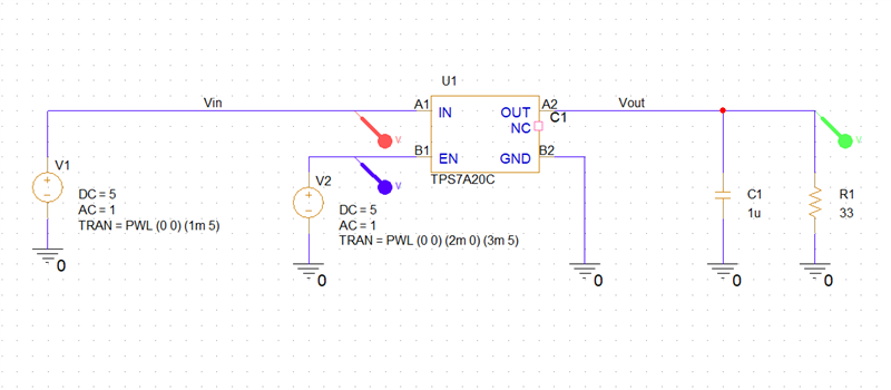
    I had a chance to test this in PSpice. I'm unable to reproduce the simulation behavior you're seeing, though it's possible this is due to a difference in the test circuit. Using this circuit: 

    and the model file you provided above, I see the following simulation results: 

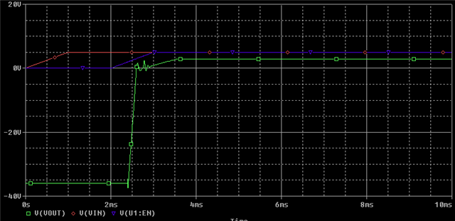
    If I replace the load resistance with a current source instead, The DC simulation result is incorrect, due to the current source pulling current from the LDO output while the LDO is disabled, but the LDO output recovers to the expected output level once it is enabled again: 

    Load current for this test was 300mA

    Best Regards,

    Alex Davis

  • To:Davis-san,

    Thank you for attention..

    We use Viruoso/spectre(cadence) environment.TPS7A20C_Pspice_models_correct_behavior_Request_2nd.pptx

    I attached my trial results .

    But could you help us ?

  • Hi Yasuda-san,

    I haven't tested this in Spectre yet, I'll test this tomorrow to see if I can track down why this issue may be occurring. 

    Best Regards,

    Alex Davis

  • Dear  Davis-san,

    I can work a little as my trial document(  How_does_it_work.ppt )  ※I attach this file.

    The cause was how to create a pspice symbol in Virtuoso(my mistake...)

    However, the results still are not good in terms of simulation characteristics.

    I have some questions in my attached file.( No1.~No.7)

    Could you answer?How_does_it_work.pptx

    Best Regards,

  • Dear Davis-san,

    As page4 of my attached file(How_does_it_work.pptx),

    Correstion :TPS7A20C Characteristics  using Pspice model(tps7a20c_trans.lib)..

    Best Regards,

  • Hi Yasuda-san,

    The TPS7A20C macromodel uses a simplified architecture. As noted in the model file, not all behaviors of the TPS7A20 are reproduced. This likely accounts for the difference in model behavior vs. characterized behavior you're seeing. 

    It appears that the modelled enable threshold is incorrect - the parameters VENB and EHYS control this threshold. Values of VENB=0.9 and EHYS=0.6 should reproduce the expected 0.9V rising and 0.3V falling thresholds for the enable input. 

    Best Regards,

    Alex Davis

  • To:Davis-san,

    Thanks to your help, I was able to control the operation using the voltage at the EN terminal. 

    Are there no fitting parameters that match the operation of the actual  each chips(TPS7A20 & TPS7a20C)  in TI?

    In terms of accuracy, we cannot actually use it unless we fine-tune it a bit more.

    Can we confirm the differences in characteristics between TPS7A20 and TPS7A20C with this macro model?

  • Hi Yasuda-san,

    This model architecture has fairly limited tuning options. The DC PSRR value, and the PSRR's first pole and zero can be adjusted, as can the reference voltage and DC output resistance. The model should show differences in PSRR between the TPS7A20 and TPS7A20C. 

    Best Regards,

    Alex Davis

  • To:Davis-san

    As you mentioned, I also believe that we need to express the difference between TPS7A20 and TPS7A20C in the model, but we do not have a good understanding of that difference. So, could you please send me the fitting parameters that match each actual chip(TPS7A20 & TPS7A20C)?

    Best Regards,

    Kenji Yasuda

  • Hi Yasuda-san,

    TPS7A20C offers improved load regulation (11mV vs. 13mV for the non-C version) and improved load transient response (compare TPS7A20 Figure 5-51 thru 5-54 to TPS7A20C Figure 5-19 thru 5-22). TPS7A20C has a slightly higher quiescent current than TPS7A20 (18.5µA max vs. 15µA max)

    Load transient and quiescent current are not accurately modeled by the macromodel architecture used for the TPS7A20 and TPS7A20C macromodels, unfortunately, so there are not parameters available that can be used to tune either behavior. 

    Best Regards,

    Alex Davis