A related question is a question created from another question. When the related question is created, it will be automatically linked to the original question.
This is actually the UCC256612 model. High voltage startup is not a feature as the model tries to focus on startup an operation over the full load range. We are working on updating this and releasing versions covering the different options available.
The Simplis model requires the SImplis simulation tool. It can't work in Tina.
The LLC topology is far too complex for a pspice based model. If we did make one, it would take forever to run. Simplis is a piece-wise linear simulator that works much faster.
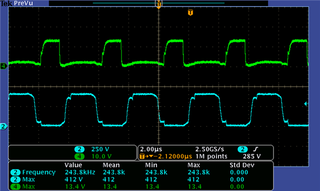
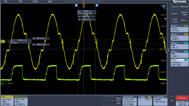
I understand, but my question is, the duty cycle of high-side and low-side vgs is only around 40% (dead time is large), how to adjust its duty cycle to be close to 50%?
The UCC25661 has adaptive dead-time control and this is a function of how you setup the resonant tank. Are you seeing this at a no-load condition or full load?
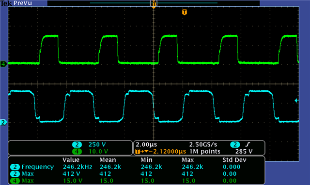
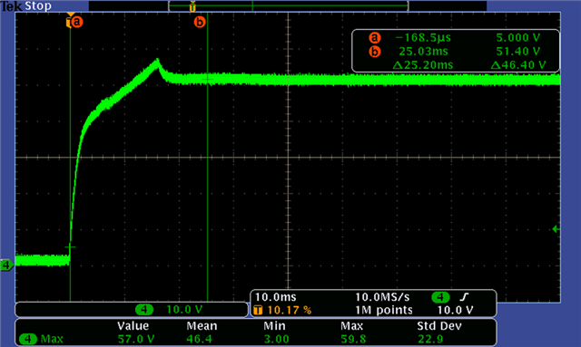
This looks like a startup waveform what is the actual deadtime you are measuring? From the shot above it looks like it is less than 1us which is normal. Have you looked at steady-state operation?
You need to look at the HO and LO pulses to see the duty cycle. Not VGS and VDS. If you look at HO and LO, you will see that the are on equal amounts of time.
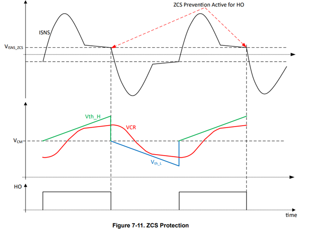
The LO and HO pulses are on for the same duration which is normal and required for resonance. What you are looking at is the dead-time which is required to allow the current in the resonant tank to reverse so the next switching cycle can be ZVS (Zero-Voltage Switched).
This is exactly what I'm curious about — why is the dead-time so large? How can I verify whether the dead-time value is correct? I’d like to reduce the dead-time because the duty cycle is too small, which leads to low voltage utilization and prevents the LLC from operating at the expected resonant frequency.
Initially, I thought the smaller duty cycle was caused by the ZCS protection feature, but based on actual measurements, that doesn’t seem to be the case.
Could you provide more methods to help me confirm whether the duty cycle is indeed too small? This could be a serious issue in the design.
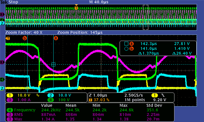
The maximum dead time is 1us. This is the adaptive dead-time is determined by looking a the slew rate on the HS pin. If you are hitting the maximum dead-time it could be that your COSS of the switch stage is too large. See Section 8.2.2.12:
This means your LI2 energy needs to be greater than the COSSV2 energy.
Can you try FETs with a lower COSS to see if it helps?