


Tool/software:
Hello EricLee
Can you please explain the technical reason to me how each of your recommended steps listed below can help in reducing the emissions.
- Make SW node copper area smaller.
- Add RC snubber between the drain and the source of the low-side MOSFET.https://www.ti.com/document-viewer/lit/html/SSZTBC7
- Populate a schottky diode in parallel with low-side MOSFET
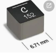
- Use shielded inductor with minimized pin lead exposure. The pin leads are hidden on the bottom side in this example.
- Locate the 'dot' (or 'bar') direction of the inductor at the SW node.
