This thread has been locked.

If you have a related question, please click the "Ask a related question" button in the top right corner. The newly created question will be automatically linked to this question.

UCC14241-Q1: RLIM Selection for UCC14241 for UCC21710 based SiC Gate Driver

Part Number: UCC14241-Q1
Other Parts Discussed in Thread: UCC21710, , UCC15241-Q1

Tool/software:

Hi,

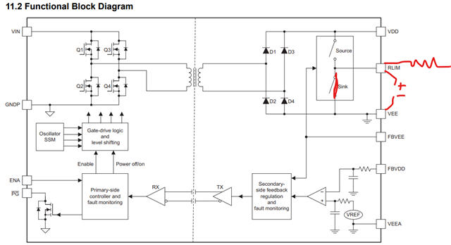
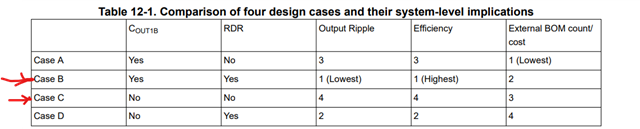
I am using the UCC14241 IC to provide dual output power rails for a SiC MOSFET gate Driver (VDD: +15V; VEE:-5V). The gate driver IC I'm using is UCC21710. Please see the excel design calculator for the UCC14241 attached.

I am trying to determine the correct value of RLIM to use based on the inputs I have provided in the excel calculator. Also note that I am implementing the single RLIM network. I am not using the RDR network.

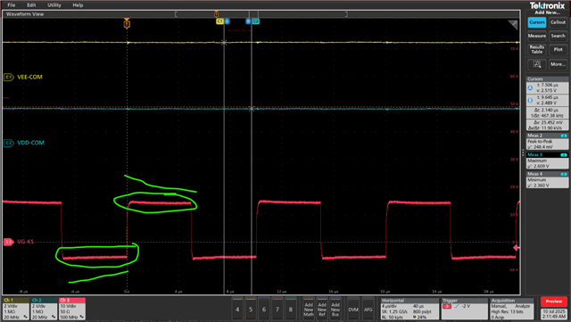
Also note that I have followed all datasheet layout recommendations for filter capacitors close to UCC14241 and UCC21710 appropriately.

Based on the above scenario and my inputs, the excel calculator suggests using the closest, smaller value to 8.2 kOhms for single RLIM.

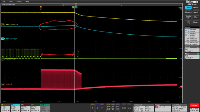
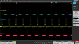
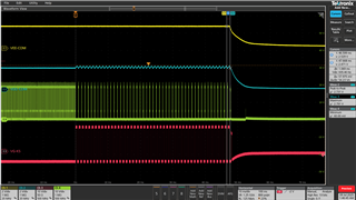
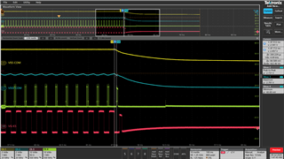
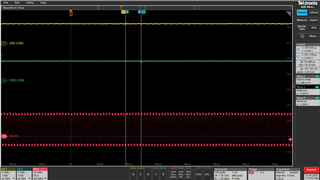
In my PCB implementation, I tested the UCC14241 circuit  with 6.2 kOhms and 8.2 kOhms. However, the VDD and VEE measured from UCC14241 are 0V and it seems to be in a fault state.

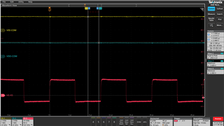
I then changed the RLIM to 1 kOhms, and it works. I am measuring +15V and -5V for VDD and VEE, as expected. This test was performed under light/no load conditions: UCC21710 is enable but PWM inputs are held low.

So, this is my question:

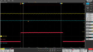
What is the maximum single RLIM I should use to minimize dissipation of UCC14241? I also want to ensure that the VDD and VEE regulation is good with 100 kHz switching frequency when gate driver is operational.

UCC1424x-Q1_Calculator.xlsx 

  • Hi Kartavya. This is a very good question. Thank you for all of the details and for providing the calculator. I've assigned your query to our UCC14241 product expert. However, they are currently out of the office but will be returning on 7/7. Thank you for your patience.

  • Based on your inputs to the Excel tool, your total power requirement is 390mW and if considering a single RLIM resistor configuration you should not exceed 8.2kΩ. I should caution that RLIM=8.2kΩ is the max value based on ideal output capacitor values and ratio and perfect balance of gate driver quiescent current. A large value of RLIM (close to 8.2kΩ) is preferred to reduce power dissipation but if the RLIM value is too large it inhibits the RLIM function being able to compensate for charge imbalance. 

    RLIM=1kΩ is giving 75mW power dissipation which is still good for 0603 size resistor. As you move much below 1kΩ the power dissipation will demand 0805 or larger case size which is where the benefit of configuring RLIM as RDR comes into play.

    Also, be careful to make sure your output cap ratio is as close to perfect as you can get. Ideally you want VDD*C_VDD=VEE*C_VEE but the further you move away from the ideal cap ratio, the more you will depend on RLIM to make up the difference a the lower value of RLIM will be necessary. Also be aware of DC bias effect on your output caps.

    Regards,

    Steve

  • Hi Steve,

    The gate drive levels I'm using are 15V, -5V.

    Based on the outputs of the Excel calculator, I found that the most optimal combination to minimize capacitor ratio deviation was to use 3.3 uF for COM-VEE and 1 uF for VDD-COM. Any other capacitor value to minimize the mismatch further is leading me to highly non-standard values.

    Given this situation, What would be your recommendation if I want to stick to an 0603 RLIM package? Do I need to migrate to the RDR network to reduce the dissipation?

    If so, I'm guessing that any standard SMD diode with V_rev > 30V should be sufficient since the current through the diode is so small (about 0.5 mA max according to the excel calculator)? 

  • If your satisfied with your output cap ratio and 1kΩ is giving consistent results then stick with that. If you can afford the PCB space and want to have the added option of RDR, I would recommend to allow for the extra R+D. For the diode we recommend a Schottky....something like BAT54

    Steve

  • Thanks a lot for the feedback, Steve.

    I conducted new tests with the MOSFET populated now, so there is a realistic load on the gate driver. Unfortunately, even with 1 kOhm, I am experiencing the same fault that is shutting down UCC14241. Please see the scope shot and updated Excel calculator attached below.

    Since I'm approaching the limit of dissipation with an 0603 package, do I now have to definitely populate the RDR circuit to resolve this issue?

    If so, could you please recommend what values would be good starting point for RLIM1 and RLIM2, because the calculator is recommending a very high maximum value at 14 kOhm and 17 kOhm respectively.

    Thanks for any advice you can share on this.

    UCC1424x-Q1_Calculator_Updated.xlsx

  • RDR may help and the values are typically something like 300-500Ω and 1-2kΩ. However, from the waveform, there seems to be something more happening here.

    1. Is the waveform the very first gate drive pulse and then the UCC1`4241 is shutting down or is it running for a while then shutting down?
    2. Interesting that the -5V seems well regulated, then the gate drive pulse switches to +15V, runs for ~150μs then shuts down. Your cap ratio is ~3:1 which is good but what is the voltage rating of your CVDD (15V applied) and CVEE (5V applied) caps? What is the effective capacitance due to DC bias - you can check this with the manufacturer.
    3. Where are the CVDD and CVEE cap physically place - they should be as close as possible to the gate driver VDD, VEE pins
    4. C_VDD-VEE caps should be placed as close as possible to the UCC14241 output pins.
    5. Make sure you allow the UCC14241 to fully regulate then turn on the gate driver PWM signal. Do not allow the gate drive to try and drive the MOSFET while the UCC14241 is still trying to soft start.
    6. When the shutdown happens can you reset the system by toggling UCC14241 EN? Can you reset the system by toggling VIN?
    7. I like the waveform you are showing but what's happening at the UCC14241 to cause this shutdown? Keep the waveform you have but also show FBVDD and FBVEE so we can see if FBVxx is causing the shutdown? Confirm if FBVDD<2.25V, then the VDD starts to shut down. If FBVxx are both valid and only drift down in response to VDD/VEE shutdown, then the issue might be on the input side?
      1. Keep the same waveform you have but shown VIN and EN measured as best you can acquire close to the UCC14241IC pins. Zoom in on the VIN at the moment the shutdown is happening and make sure there are no dips in VIN where the VIN might droop below 21V

    Steve

  • Hi Steve,

    Thank you for the response. I have been concerned about the capacitor ratings as your first few questions indicate. PLease see some of the responses below:

    1. With the MOSFET acting as load on the gate driver, this is happening after the first pulse. Under no load conditions (MOSFET unpopulated), this affect was occuring after 2-3 pulses.

    2. The parts I'm using are Samsung CL10B105KB8NQNC  for CVDD and TDK CGA4J1X7R1V335K125AC for CVEE. But these are X7R and the Samsung datasheet shows a very poor DC bias characteristics. Please see curve below from datasheet:

    3. CVDD (1 uF) and CVEE (3.3uF) are placed at less than 3 mm distance from the Gate Driver IC pins

    4. CVDD-VEE (2.2uF || 0.1 uF) is also placed at less than 3 mm distance from UCC14241 pins  

    5. I have ensured that gate driver PWM signal is only turned on after UCC14241 is regualting Vdd and Vee, and also ensured that the PGOOD signal is indicating a power good condition.

    6. After the shutdown occurs, I am able to easily reset UCC14241 by toggling EN, which resets to the default 15V VDD, and -5V VEE. I measured this across CVDD and CVEE. Also, Vgs is at the expected -5V during the normally off state. 

    7. After the shutdown occurs, PGOOD is pulled high even though EN is high from my MCU.

    Based on my responses above, could a quick test with stacking more of the X7R caps in parallel improve performance? Perhaps even replacing them with Class 1 caps?

  • In addition to my response below, I ran another test.

    I replaced CVDD with 3.3 uF and CVEE with 10 uF to see if the higher capacitance helps.

    To summarize:

    Before: CVdd = 1 uF; CVEE = 3.3 uF

    Now: CVDD = 3.3uF; CVEE = 10uF

    As you can see in the scope capture below, now the shutdown occurs midway through the second pulse. So the higher capacitance helped a little, but not by much. Also, with the new capacitors, I checked that the DC bias variation is within 15% at 15V.

    Please also note that the switching frequency for this test was only 1 kHz, which is far below my target switching frequency of 100 kHz.

    The RLIM I am using currently is 1 kOhm. I have also attached the updated Excel calculator with the new capacitance values.

    I could try to reduce the RLIM to 500 Ohms and use an 0805 component. But I'm not sure if I'm missing something.

    Given my PCB implementation, it is not quick/easy to monitor FBVEE and FBVDD. Could you please advice on whether the results in my previous and current response provide any insights for further action?

    If not, I will try to probe FBVEE and FBVDD as best as possible.

    7444.UCC1424x-Q1_Calculator_Updated.xlsx

  • What does RLIM look like? What's up with the "hump" on VDD during the turn on pulse - can you look at the UCC14241 output at the same time you are showing the gate drive pulse? You have an 8-channel scope but you are only showing a single channel. Lets grab the most information we can during the debug? Even though the cap ratio is close to ideal, there could still be the chance for charge imbalance if there are any additional loads on VDD and/or VEE not accounted for. Besides the gate driver, are there any additional loads on VDD and/or VEE? If no loads are known, then I would recommend to replace RLIM with RDR, although seeing the same issue with the single RLIM=500Ω is concerning.

    Steve

  • Hi Steve,

    Thanks a lot for the detailed feedback.Please note that the gate driver for a single SiC MOSFET is the only load on the CC14241 being tested.

    To clarify, after changing RLIM to 500 Ohms, I am able to continuously switch at 50 kHz and performance is within expectations. Here, the MOSFET is still populated and serves as a load on the gate driver. Summary of passive component values for this test: RLIM = 500 Ohms; CVDD = 3.3 uF; CVEE = 10 uF. Please note that I had increased CVDD and CVEE before changing RLIM to 500 Ohms.

    I ran the test at 100 kHz with the same configuration as above. However, after a few pulses, UCC14241 shuts down. As per your recommendation, I have monitored FBVDD - VEE; FBVEE - VEE; RLIM-VEEA; and MOSFET Gate voltage. Please see the scope captures in the zip file attached to this response.

    It looks like FBVEE is continuously rising to 2.75V. At this point, FBVEE and FBVDD start to decay. I wonder if this is the shutdown process beginning. Finally, when FBVDD and FBVEE are at ~1.9V and 2.3V, UCC14241 seems like it completely shuts down.

    Does this indicate that I should reduce my CVDD and CVEE back to original values since I reduced RLIM to 500 Ohms? The old values were 1 uF and 3.3 uF, respectively.

    Or do I need to populate the RDR circuit first?

    Would you happen to have any advice on this?

    Please note: I also included a scope capture in the zip folder, showing VDD-COM and VEE-COM relative to MOSFET gate voltage.

    For your convenience, I have also re-attached the excel calculator with the passive component values I used for the tests above.

    Scope Captures.zip

    8004.UCC1424x-Q1_Calculator_Updated.xlsx

  • Thanks for the plots, these are good. 

    It looks like FBVEE is continuously rising to 2.75V. At this point, FBVEE and FBVDD start to decay.

    FBVDD looks good but the FBVEE=2.75V is triggering FBVEE OVP and causing the IC shutdown. The RLIM cannot help to resolve the charge imbalance and you can see that before any PWM pulses appear, RLIM is active but the UCC14241-Q1 is sort of idle during this time because there is no load. As soon as the PWM is introduced, FBVEE begins a linear rise. We can see it clearly on C2 (2V/div) but it's not showing on C3 (10V/div) because there is not enough voltage scale resolution to show a 250mV change. In any case, the RLIM is inactive while FBVEE is rising and what would be nice to have is FBVDD, FBVEE, VDD-COM and COM-VEE. I expect that COM-VEE is increasing (~5.5V) and VDD-COM (not directly regulated by FB) is decreasing (~14.5V) but from the gate drive signal it's hard to tell what the actual rail voltages are doing in response to FBVxx?

    I'm not sure what is causing this rise in FBVEE? Extra power draw/imbalance, partial cross conduction if driving half-bridge, some mismatch load between VDD and VEE, partial damaged MOSFET/SiC/IGBT? Are you driving a half-bridge and is there a measurable dead-time maintained between HS-LS? Otherwise, change the MOSFET, change the UCC14241-Q1 and maybe order and try UCC15241-Q1?

    Steve

  • Hi Steve,

    Thank you for your feedback. The topology is a non-synchronous buck converter, and I am only driving the high side switch. The low side device is just a diode. Also, "Scope_Capture5" in the attached zip folder in my previous response, shows VDD-COM and VEE_COM. The behavior is as you expected.

    Based on your response, I have a few questions. Please see below:

    Q1. Why is RLIM getting disabled before the FBVEE OVP is triggered? It seems that as soon as the PWM signal is provided, RLIM stops switching. To further understand this, I re-ran the test at 50 kHz instead of 100 kHz. Please see the scope capture below.

    From the above scope capture, RLIM still doesn't switch at all. However, at 50 kHz, at least I am able to switch MOSFET gate continuously. I also noticed that FBVEE is relatively stable and stays around 2.65 V. What do you think is happening? Will the RDR circuit be helpful in any way here? 

    Q2: CVDD and CVEE are 3.3uF and 10 uF, respectively. Is this capacitance very large and should I reduce them such that CVDD is 1 uF and CVEE is 3.3uF? Could it be that there is stored charge build up and CVEE is not discharging sufficiently?

    Q3: What would be the benefits of UCC15241 over UCC14241? Is it just the slightly higher power rating or anything else?

    Q4: Is the external circuit configuration identical to UCC14241? And can I use UCC15241 as a drop in replacement?


    EDIT: I re-tested at a significantly lower PWM switching frequency of 1 kHz. The RLIM switching is at least active now, and looks better. Please see scope image below. It seems that the issue is apparent at higher PWM frequencies (when gate driver load is higher). However, after a few minutes, the GDPS shuts down in the same faulted state as before. Does this indicate anything for troubleshooting?

  • Interesting that you are seeing shutdown at 100kHz, where the required power is highest and then you are seeing shutdown at 1kHz, where the required power is lowest but at 50kHz, the UCC14241 is able to operate continuous.

    1. 100kHz: Ripple is low but power is high
    2. 50kHz: Ripple is still low and power seems ok
    3. 1kHz: Ripple is high and power is low

    Q1. Why is RLIM getting disabled before the FBVEE OVP is triggered? It seems that as soon as the PWM signal is provided, RLIM stops switching. To further understand this, I re-ran the test at 50 kHz instead of 100 kHz. Please see the scope capture below.

    A1: RLIM responds to FBVxx and, from the previous waveform I marked up, you can see that as soon as the PWM beings switching, the FBVEE is linearly increasing from 2.5V to 2.75V then shutting down. RLIM responds by compensating to sink as much current as possible from COM to try and pull FBVEE back into regulation. The time you see RLIM "stop switching" is when the low-side internal RLIM "Sink" switch is fully on because FBVEE is continuing to rise. You are measuring RLIM at the point I marked below as +/- and when you see RLIM stop switching, you are really measuring a short at RLIM-VEE

    Q2: CVDD and CVEE are 3.3uF and 10 uF, respectively. Is this capacitance very large and should I reduce them such that CVDD is 1 uF and CVEE is 3.3uF? Could it be that there is stored charge build up and CVEE is not discharging sufficiently?

    A2: The cap ratio is what matters. Make sure to follow the cap value recommendations coming from the Excel.


    Q3: What would be the benefits of UCC15241 over UCC14241? Is it just the slightly higher power rating or anything else?

    A3: Higher power capability which may be part of the issue when operating at 100kHz

    Q4: Is the external circuit configuration identical to UCC14241? And can I use UCC15241 as a drop in replacement?

    A4: Yes, both are p2p compatible and drop in replacements with no external circuit changes needed.

    Go ahead and try RDR and Cout1b, Case B below. Right now you are using Case C....ripple is highest, efficiency is lowest and the limitation on RLIM is such that it cannot compensate whatever is causing the charge imbalance. Try RDR on UCC14241 first, then maybe try swapping UCC14241 with UCC15241.

    Steve

  • Hi Steve,

    Thanks for the suggestions. I will try with RDR and potentially swapping with UCC15241.

    However, to clarify, I am currently using Case A. I have Cout1B placed close to gate driver IC (UCC21710) and Cout1 placed close to UCC14241.

    Does the above clarification affect your recommendation in any way? Seems like RDR should still help.

  • Thanks Steve,

    If I stick with 500 Ohms for RLIM1, is RLIM2 at 10k too large? Or should I cap this at 3.3K, similar to the Excel calculator suggestion for RLIM1?

    For context, with updated values, the excel calculator suggests a max of 8.2k for RLIM1 and ~14k for RLIM2

  • We already know that 500Ω in the sink path is not low enough bit I would recommend to start with this and verify you get similar results as your previous testing when using a single RLIM resistor. For the source path, start with 1kΩ. Be prepared to lower 500Ω and hopefully be able to increase 1kΩ. Test it and determine optimal values for reliable operation vs power dissipation.

    Steve

  • Hi Steve,

    So I ran a couple of tests yesterday. With an RDR (RLIM1 = 1 kOhm, RLIM2 = 500 Ohm) for UCC14241, I was able to switch at 100 kHz continuously. I also left the gate driver running for more than 30 minutes to ensure that no other issues are being hidden. FBVEE and FBVDD stayed around ~2.5V as well. This indicated to em that the regulation was also performing well. Please see some high level scope captures below:

    However, I tried to repeat the above test today to ensure that the gate driver is operating reliably. Unfortunately, at 100 kHz, I'm running into the same issue as before. FBVEE climbs to ~2.7V and UCC14241 shuts down.

    As per your recommendation, continued tuning the RLIM values. TO summarize the new setup, here are the main component values: COUT1 = 2.2 uF; COUT1B = 2.2 uF; Cout2 = 1 uF; Cout3 = 3.3uF; RLIM2 = 200 Ohms (sink) and RLIM1 = 1 kOhms (source). With this setup for UCC14241 and RDR populated, I am able to switch at 1 kHz, 50 kHz, and 100 kHz as of now.

    I am also monitoring FBVEE and FBVDD. At 1kHz switching frequency (conservative scenario for ripple), the peak - peak ripple on both is less than 75 mV (ripple frequency seems to be around 35 kHz). Please see the zoomed-in scope images below for the 1 kHz case:

    So, my main question is this: Given the relatively non-repeatable/unreliable operation I observed based on RLIM values, how can I ensure that UCC14241 will operate reliably if I freeze the current RLIM values? Any recommended performance metrics that I should target?

    Also, do you still recommend swapping the IC with UCC15241?

    Any advice you can share based on the above results would be very much appreciated.

  • Ripple still looks a bit large - how about trying to increase COUT1 from 2.2μF to something like 4.7μF-10μF? Also, the gate drive waveform looks like it has a very slight slope (circled in green below) which, if it does, I do not quite understand because a slope in the gate drive VDD/VEE should show as a slope in the VDD-COM and COM-VEE but the voltage rails themselves do not show this slope - why? This hints that the gate drive capacitors might not be ideal in their placement and/or routing? Closest to the gate driver pins, no vias with direct tracks or copper pours are preferred. Maybe zoom in on the green circled areas of the gate drive waveform and switch to AC coupling on the voltage rail waveforms and zoom to see if this slope is evident on 1 or more waveforms?

    Steve