Other Parts Discussed in Thread: LM5088, LM5148
Tool/software:
Subject: LM5088-1 DC/DC Converter Design – Request for Support
I’ve developed a DC/DC step-down converter design using the LM5088-1 for 48V to 24V at 5.5A. The calculations were performed using TI’s Webench Power Designer, and I also verified component values with the LM5088 Quick Start Calculator.
The results from both tools are comparable.
However, I’m currently facing three issues:
- Significant ringing at the switching node
- Jitter on the falling edge
- Ripple on the output when the converter is unloaded
The low-frequency ripple is present up to a load of approximately 200mA. At higher currents, up to 5.5A, the output is stable.
Attached are scope images showing:
- 1.Ringing at the switching node (measured with a Tektronix bayonet probe)
- 2. Jitter at the switching node
- 3.Output ripple voltage at a 20mA load
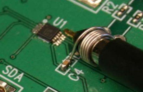
The PCB layout is similar to the evaluation board for the LM5088.
Could you please advise on possible solutions or improvements?
Fig. 1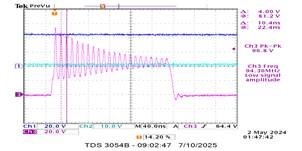
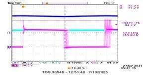
Fig. 2
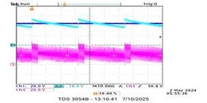
Fig. 3
The light blue trace represents the ripple on the 24V output voltage, while the purple trace shows the voltage at the switching node.