LM5046: LM5046 implementation questions

Part Number: LM5046
Other Parts Discussed in Thread: UCC28950

Tool/software:

Hi,

I read the LM5046 datasheet and while using the provided XLSX calculator I noticed something strange:

When calculating R1 R2 R3 i get very different results when compared to datasheet formulae. 

Vin is between 300-410Vdc 390V nominal ( with a lot of room for when APFC is not started yet and to account for shrt mains hiccups)and Vout 50V

I set the Vth to 10V hysteresis and that results in 500k and that is ok.

I set OVP to 440V , UVLO to 300V, here the results are very different. 

With manual math i get 2k15 and 1k4 and that results into 750 and 1k42 for 3 resistor setup.

With XLSX calculator i get 420 1k62 for 3 resistor setup.

This is a large difference and I am not sure why this is happening. Yes 1k42 and 1k62 are very close and rounding might play a large role here BUT 750 vs 420 is a large difference in terms of ratio.

On another note i didn't find a lot regarding how to calculate the transformer primary inductance so i used : https://www.ti.com/lit/an/slua560d/slua560d.pdf?ts=1752674969435&ref_url=https%253A%252F%252Fe2e.ti.com%252F  Is this ok? 

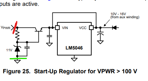
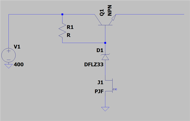
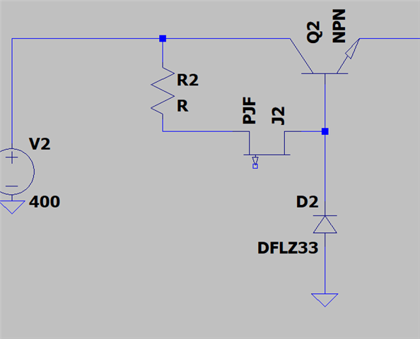
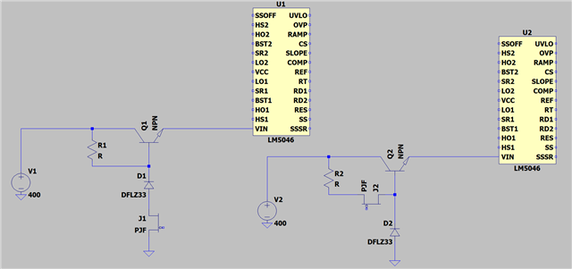
Regarding the high voltage start-up from page 30 of the datasheet: 

Would there be any problems if i do it is 2 stages?

As in 400Vdc -> 80Vdc with external NPN -> IC input ( and then generate 13V from a transformer auxiliary winding. 

In the datasheet the internal linear regulator in entirely bypassed while i was considering using it since 300-320V drop on a single NPN seems a bit much.

I will do some simulation but generally would this be ok? 

How can i stop the start up circuit? Could a low side JFET under the Zener diode do the job?

 Best regards,
Robert

  • Hi,

    Please provide the calculator with your numbers filled in then indicate which cell values you are referring, as the calculator from ti.com does not seem show R1, R2 and R3.

    Also, provide your calculation development (take a picture of your draft paper to show how you come out the numbers on which equations etc).

    I am not sure what is your two stages - please sketch a drawing to show your intention to do. 

    To stop your start up circuit, a simple way is to disconnect it from your circuit to open the VCC then the IC stops working. If provide more specific details and draw a diagram to show what you want to do we can see if better suggestions. 

  • Hi,

    UCC28950 and LM5046 are on same topology phase shifted full bridge so ok to design the inductance on a same approach.

  • HI,

    In the TI calculator:

    R1 is R6 ( cell C3) this is fine it is 500k 

    OVP , R3 is R9 ( cell C4) 

    My math : ( 1.25 * 500*10^3 ) / ( 430 -1.25 + 20*10^(-6)* 500*10^3 ) like in the datasheet, and i get 1424.5 so about 1.4k while TI calculator gives 1.6k 

    UVLO R2 is R7 ( cell C9) 

    My math : ( 1.25 * 500*10^3 ) / ( 300 -1.25 - 20*10^(-6)* 500*10^3 ) like in the datasheet, here i get 2164.5 so 2.16k 

    From this we need to subtract the previously calculated resistor 2164.5 -  1424.5 => 740 but here TI calculator ended up with 340 . 

    I am not sure from where the discrepancy is but checking the TI the cell formulae they also seem correct.

    Regarding the 2 stages, maybe my explanation was not clear enough, here is another take on that:

    Stage 1: NPN linear regulator from 400V to 80V . Just like page 30 from datasheet , chapter 8.2.2.6

    Stage 2: Internal HV start-up built into the LM5046 IC

    In chapter 8.2.2.6 the input voltage is reduced to 11V directly and the internal HV Start-up is bypassed.

    I am afraid that the external NPN will heat up to much and that is why I was considering spreading the power dissipation across 2 components.

    Regarding start-up disconnection: 

    Here is the image from the proposed datasheet circuit I was thinking about eliminating the constant power draw through the resistor and Zener diode by disconnecting them either on the low side or high side. I want to to be solid state and not require that many external discrete components. I wad considering P-chan JFET on the low side ( green line) since they are conducting by default with 0V on the gate and then maybe turn it off with a op amp used as a comparator. I can power the op amp from the Vaux.

  • Hi,

    I am not seeing the same. Please provide your excel sheet to help discussion. 

    I am seeing R6 = 100k, different from what you say. I think it is likely due to different specs which I think you should provide your excel sheet to help us on the same page.

  • Hi,

    That is normal since default hysteresis is 2V and i set it to 10V. I mentioned that R6 is 500k .

    Not sure how to attach files and what types are ok to upload here but i can provide the data i used.

    V(in)min   300.00 V Min Input Voltage
    V(in)nom   390.00 V Nominal Input Voltage
    V(in)max   400.00 V Max Input Voltage
             
    Vout   48.00 V Output Voltage
    DVOUT   75.00 mV Max Output Voltage Ripple
    Iout(max)   5.50 A Max Output Current
    Iout(min)   0.50 A Min Output Current
             
    UVLO   310 V Under Voltage Lock Out
    OVP   440 V Over Voltage Shutdown
    DVH   10 V Input Voltage Hysteresis
             
    f   500 kHz LM5046 Clock Frequency

    Best regards,

    Robert

  • Hi,

    Again, please provide the excel sheet which shows different from your hand calculation. We need to see the excel sheet to find if all filled in numbers are possibly a reason to cause the differences. We cannot help if you do not want to provide that excel sheet as we cannot figure out what else possible making things different between your calculations and excel calculations.

  • Hi,

    It should be attached below.SLUC500_LM5046_V1.xlsx

    Best regards,

    Robert

  • Hi,

    OVP , R3 is R9 ( cell C4) 

    My math : ( 1.25 * 500*10^3 ) / ( 430 -1.25 + 20*10^(-6)* 500*10^3 ) like in the datasheet, and i get 1424.5 so about 1.4k while TI calculator gives 1.6k 

    430 is not the same in your excel which shows 400.

    When change D5 to 430, excel gives R9 = 1.49k

    Another error in your calculation is that "+" should be "-" based on equation (1)

    ( 1.25 * 500*10^3 ) / ( 430 -1.25 + 20*10^(-6)* 500*10^3 ) = 


    From this sample check, it looks your calculation has quite errors. I suggest you make carefully reviewing of your calculations to correct all possible errors in your calculations. After that if you still see differences, please show like what I show above to list side by side to point out where you have differences.

  • HI,

    OPS , THX for the help.

    Regarding the low side JFET what do you think?

    Also did any of the XLSX parameters look off to you ?

    Best regards,

    Robert

  • Hi,

    I am not sure what you mean low side JFET? Please provide detail.

    Excel file has been used by other designers inside and outside TI, it should be good, but if you see something not in line with your calculations, you need to provide the detail like what I did. As the file was checked before the release, we take the file as good and correct. Unless you can point out and provide details. So far, I see your errors not the file. So you need to be specific and details oriented.

  • Hi,

    Regarding the p Jfet this is as of now just an idea, i was thinking of something like this:

    R1 Q1 are like in the 8.2.2.6 chapter, i added J1 a Jfet since that type is default conducting and i was thinking that i can reduce the power loses through R1 D1 ( after the SMPS is running and there is no longer a need for this part of the circuit to be active).

    Regarding control, i was thinking of a few comparators or op amps. 

    JFET might not be the best choice but i am very flexible here, other depletion mode device could also be used.

    Alternatively i was thinking of this:

    Same concept but potentially easier to drive J2 

    Then again maybe i am trying to reinvent the wheel so i must ask: 

    Is there any alternative high voltage start up circuit that i recommended by TI? Yea the presented one is simple cheap and probably reliable but will constantly bleed current and thus somewhat a lot of power at 400Vdc. 

    I know there is a special FET from Microchip for high voltage start up, so i was wandering if TI has something similar or a IC solution. 

    Best regards,

    Robert

  • Hi,

    I am not able to understand what you want to do. Please draw these into the circuit with LM5046 to see if we can understand. Note we are supporting LM5046 while not sure if we can help your new ideas. We can try but you need to draw your own idea as a circuit with LM5046. Note we may not be able to help for your new ideas.

  • Hi,

    Sorry for the late reply i got caught some other stuff.

    Attached there is the schematic of what i was thinking : 

    Also do you recommend some RC snubber over the Secondary MOSFET or not ?

    Best regards,

  • Hi,

    These just convert 400V to a voltage in the Vin range of LM5046, yes it is ok. But note if Vin = 400V, you need to use external driver to tolerate the voltage since LM5046 HS1 and HS2 voltage ratings are not able to tolerate 400V.

    These JFETs in your drawing do not have gate signal - how you make them on/off control?

  • HI,

    Regarding the gate drivers i know TI has some half bridge gate drivers that can tolerate 12-15V input signals, it is also a standard pinout, so in this front i already did my homework, this is part of the reason why i responded late.

    As for the JFET control I think i mentioned that i was thinking of using some op amps for that , at this voltage there are only N type so I am no longer sure it can ge done that easy. 

    In current mode control i noticed there is somewhat a discrepancy between how the current sense load resistor in calculated between the UCC application note and TI XLS calculator. For me it is 60ohm using XLS ( here it is 75% of ideal* steady state resistor for max current) .
    IF i use the formula form the UCC28950 ( also change the peak current on CS pin voltage value from 2V to .75V) then i get 38.5 OHM.

    But for the LM5046 the slope is with current 0-100uA through slope resistor R13 in XLS and that translates to 0.24V for me , and if i do the math with this value i get 35.66 OHM.

    Asking since i did a bit of test simulations and there were problems with 4A load ( while max is 5.5A ) with 48V out, and it was down to the CS pin ( RES cap was charging so that is why i started digging down this path).

    Also I am aware that i am using a much higher  input voltage then other designs so i sort of guess the current through my primary is relatively low and the slope is a large amount of the CS pin trigger limit.

    Best regards,

    Robert

  • Hi,

    If you see difference please list side by side where exactly you see and explain in detail where the difference is so we can check to find how the difference is made.

  • HI,

    Difference is simple: in XLS calculator there is a simple formula, while in this: https://www.ti.com/lit/an/slua560d/slua560d.pdf?ts=1752674969435&ref_url=https%253A%252F%252Fe2e.ti.com%252F 

    There is a much longer formula. When comparing results there is a noticeable diff 60 VS 36/39 ohm .
    When Simulating i noticed that 60 ohm does not start up with 5A load but with 36 or 39 it is ok.

    Best regards,

    Robert

  • Hi,

    I am not able to know where is where and which is which from your message. Please indicate which formular and where it is in each document such as which cell, which page, which equation with its caption. I need to know these to know what you mean to help find and compare.

  • 0312.SLUC500_LM5046_V1.xlsxHI,

    In the XLS the formula is in cell C62 , cell content  =0.75*(Specifications!D24)/Calculations!C60 

    the 0.75 is some sort of derating/compensation , the rest is a extreme steady state value.

    As for the UCC28950 application note, it is chapter11 , page 12 
    https://www.ti.com/lit/an/slua560d/slua560d.pdf?ts=1752674969435&ref_url=https%253A%252F%252Fe2e.ti.com%252F  
     I only changed the UCC28950 values to the values from the LM5046.

  • Hi,

    Excel C62 looks ok and good to me to specify the current sense transformer output resistor value. 

    I am not sure where you get the issue on UCC28950 application note. Please point out which equations on page 12 that you think need to change.

  • Hi,

    Maybe this context was lost o i forgot to mention it:

    I simulated this DC-DC in spice using nominal input and output voltages and i noticed that at low load it is all ok but at 4-5A  ( 75-90% ) of max load there were problems. Or rather the SMPS would start work ok for a few ms then stop and restart. 

    I tried changing the compensation network and increasing the soft start cap but it did not help, then i looked into the current sense circuitry and after some more testing ( a lot more since i tried to filter noise here and there) i found out that the RES pin capacitor was charging C25. and then i started investigating.

    I used https://www.ti.com/lit/an/slua560d/slua560d.pdf?ts=1752674969435&ref_url=https%253A%252F%252Fe2e.ti.com%252F as a reference for my math and ended up with 36-39 ohm for   the current sense transformer output resistor value, while the TI calculator for my IC said 60 ohm.

    With 60 OHM it was not working so i tried with both 36 and 39 and it did work, or rather the SMPS started as expected and didnt restart.

    Then i wrote here to notify TI about this since maybe I am not the first one experiencing this.

    Best regards,

    Robert

  • Hi,

    I am not sure I understand your need. But it looks you want to mention your resistor value calculated is 39-ohm and TI is 60-ohm. But the calculator looks using a current transformer. It would be helpful you can show where is in the excel and how is your calculation to help understand where the difference is from and if it needs to make correction. At now, I am not able to follow your findings as it looks many defaults not provided.