This thread has been locked.

If you have a related question, please click the "Ask a related question" button in the top right corner. The newly created question will be automatically linked to this question.

LP8764-Q1: I2C registers read 0

Part Number: LP8764-Q1

Tool/software:

I found two E2E threads accurately describing my issue, but neither one has a resolution.

https://e2e.ti.com/support/power-management-group/power-management/f/power-management-forum/1334146/lp8764-q1-i2c-issues-with-custom-pcb

https://e2e.ti.com/support/power-management-group/power-management/f/power-management-forum/1335380/lp8764-q1-target-device-on-project-pcb-does-not-respond-to-i2c-reads

In my case I have a custom board Implementing the lp876440C0.

We developed custom firmware and loaded it to the device.  We have done this successfully on 6 prototype boards for this project.

While debugging other issues on the board I did one of dozens of power cycles, but after this power cycle the lp8764 reports 0x00 for all I2C register reads.

We have the lp87664 connected to an on board microcontroller I2C port we use for programming and monitoring.  On every power cycle we verify that the lp8764 has the proper firmware before we enable its supplies.

This worked dozens of times until it didn't.  We only programmed the NVM on this device once, and that was days ago and multiple power cycles ago.  We do change the I2C address to 0x48 during NVM reconfiguration.  This has always worked fine and helps us recognize un-programmed devices.

I can watch the I2C bus on a logic analyzer.  The lp8764 is the only device on this i2c bus.  The lp8764 still Acks the I2C writes and reads appropriately and drives SDA low at the appropriate time during reads, so it is not completely dead.

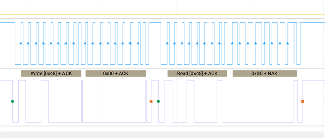
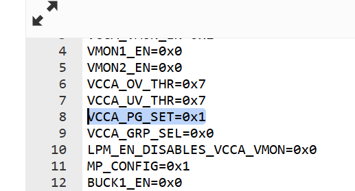
I can scan every address on the I2C bus.  Addresses 0x12, 0x48, 0x49, 0x4A, and 0x4B are the only address that Ack a write.  They all reply with 0x00 when I try to read register 1.

Did either of those other posts generate any answers to how it gets in this mode?

Any other things I can test while I have it instrumented, before we just replace the part?

  • Hi Barry,

    Can you share the full long part number of the LP8764 so we know what is supposed to be programmed into it? Or what NVM did you load, could you share the .json or files? 

    -Katie

  • Katie, thank you for considering our issue.

    Just as quickly as the issue arrived, it went away.

    I increased the supply voltage from 4.3V to 4.6V and rebooted again.  Everything worked fine after that last night and is still working today.  I cannot imagine the supply voltage is the issue.  We have other systems that use this part at 3.3V just fine.  I was just trying anything that is easy to try.

    Attached are the NVM files we used to program the device.  I did not re-program the NVM before it failed or after it failed.  Seems like the issue is somewhere else, but I am happy for you to review our configuration if you have time.

    I sort of wonder if we are beginning the first I2C request too soon after power up and corrupts the I2C handler.  Our MSPM0 processor comes up very quickly and checking the PMIC is the first thing it does.  I doubt the other engineers experiencing this issue were querying I2C that early.

    Obviously this is a scary failure mode.  It would be great to understand the root cause.

    CUSTOMER_NVM_ID=0xa3
    VMON_DEGLITCH_SEL=0x1
    VCCA_VMON_EN=0x1
    VMON1_EN=0x0
    VMON2_EN=0x0
    VCCA_OV_THR=0x7
    VCCA_UV_THR=0x7
    VCCA_PG_SET=0x1
    VCCA_GRP_SEL=0x0
    LPM_EN_DISABLES_VCCA_VMON=0x0
    MP_CONFIG=0x1
    BUCK1_EN=0x0
    BUCK1_FPWM=0x0
    BUCK1_FPWM_MP=0x0
    BUCK1_VMON_EN=0x0
    BUCK1_VSEL=0x0
    BUCK1_PLDN=0x1
    BUCK1_RV_SEL=0x0
    BUCK1_SLEW_RATE=0x4
    BUCK1_ILIM=0x2
    BUCK1_VSET1=0x5f
    BUCK1_VSET2=0x5f
    BUCK1_OV_THR=0x7
    BUCK1_UV_THR=0x7
    BUCK1_GRP_SEL=0x2
    BUCK1_RESET=0x0
    BUCK1_FREQ_SEL=0x1
    BUCK1_SEL_NEG_OCP_HYST=0x0
    BUCK1_SEL_POS_OCP_HYST=0x1
    BUCK1_SEL_ISENSE_SLOPE_COMPENSATION=0x3
    BUCK1_SEL_VOUT_ADC_LEVEL=0x0
    BUCK1_SEL_PHASE_SHEDD=0x0
    BUCK1_SEL_PHASE_ADD=0x1
    EN_LOAD_COMP_BLANK=0x1
    BUCK1_SEL_OUTPUT_CAPS=0x1
    BUCK1_SEL_RAMP=0x1
    BUCK1_EN_P_10M_BODY_DIODE=0x1
    BUCK1_DOUBLE_PFM_PULSE=0x0
    BUCK1_CHANGE_2MHZ_BELOW_0V5=0x0
    BUCK1_EN_RADAR_MODE=0x0
    BUCK1_SEL_FB_FILTER=0x3
    swc_buck_hiz_1=0x0
    BUCK2_EN=0x0
    BUCK2_FPWM=0x0
    BUCK2_VMON_EN=0x0
    BUCK2_VSEL=0x0
    BUCK2_PLDN=0x1
    BUCK2_RV_SEL=0x0
    BUCK2_SLEW_RATE=0x4
    BUCK2_ILIM=0x2
    BUCK2_VSET1=0xd5
    BUCK2_VSET2=0xd5
    BUCK2_OV_THR=0x7
    BUCK2_UV_THR=0x7
    BUCK2_GRP_SEL=0x2
    BUCK2_RESET=0x0
    BUCK2_FREQ_SEL=0x1
    BUCK2_SEL_NEG_OCP_HYST=0x0
    BUCK2_SEL_POS_OCP_HYST=0x1
    BUCK2_SEL_ISENSE_SLOPE_COMPENSATION=0x2
    BUCK2_SEL_VOUT_ADC_LEVEL=0x0
    BUCK2_SEL_OUTPUT_CAPS=0x1
    BUCK2_SEL_RAMP=0x1
    BUCK2_EN_P_10M_BODY_DIODE=0x1
    BUCK2_DOUBLE_PFM_PULSE=0x0
    BUCK2_CHANGE_2MHZ_BELOW_0V5=0x0
    BUCK2_EN_RADAR_MODE=0x0
    BUCK2_SEL_FB_FILTER=0x3
    swc_buck_hiz_2=0x0
    BUCK3_EN=0x0
    BUCK3_FPWM=0x0
    BUCK3_FPWM_MP=0x0
    BUCK3_VMON_EN=0x0
    BUCK3_VSEL=0x0
    BUCK3_PLDN=0x1
    BUCK3_RV_SEL=0x0
    BUCK3_SLEW_RATE=0x4
    BUCK3_ILIM=0x2
    BUCK3_VSET1=0xf3
    BUCK3_VSET2=0xf3
    BUCK3_OV_THR=0x7
    BUCK3_UV_THR=0x7
    BUCK3_GRP_SEL=0x2
    BUCK3_RESET=0x0
    BUCK3_FREQ_SEL=0x1
    BUCK3_SEL_NEG_OCP_HYST=0x0
    BUCK3_SEL_POS_OCP_HYST=0x1
    BUCK3_SEL_ISENSE_SLOPE_COMPENSATION=0x2
    BUCK3_SEL_VOUT_ADC_LEVEL=0x0
    BUCK3_SEL_PHASE_SHEDD=0x0
    BUCK3_SEL_PHASE_ADD=0x1
    BUCK3_SEL_OUTPUT_CAPS=0x1
    BUCK3_SEL_RAMP=0x1
    BUCK3_EN_P_10M_BODY_DIODE=0x1
    BUCK3_DOUBLE_PFM_PULSE=0x0
    BUCK3_CHANGE_2MHZ_BELOW_0V5=0x0
    BUCK3_EN_RADAR_MODE=0x0
    BUCK3_SEL_FB_FILTER=0x3
    swc_buck_hiz_3=0x0
    BUCK4_EN=0x0
    BUCK4_FPWM=0x0
    BUCK4_VMON_EN=0x0
    BUCK4_VSEL=0x0
    BUCK4_PLDN=0x1
    BUCK4_RV_SEL=0x0
    BUCK4_SLEW_RATE=0x4
    BUCK4_ILIM=0x2
    BUCK4_VSET1=0xb2
    BUCK4_VSET2=0xb2
    BUCK4_OV_THR=0x7
    BUCK4_UV_THR=0x7
    BUCK4_GRP_SEL=0x2
    BUCK4_RESET=0x0
    BUCK4_FREQ_SEL=0x1
    BUCK4_SEL_NEG_OCP_HYST=0x0
    BUCK4_SEL_POS_OCP_HYST=0x1
    BUCK4_SEL_ISENSE_SLOPE_COMPENSATION=0x3
    BUCK4_SEL_VOUT_ADC_LEVEL=0x0
    BUCK4_SEL_OUTPUT_CAPS=0x1
    BUCK4_SEL_RAMP=0x1
    BUCK4_EN_P_10M_BODY_DIODE=0x1
    BUCK4_DOUBLE_PFM_PULSE=0x0
    BUCK4_CHANGE_2MHZ_BELOW_0V5=0x0
    BUCK4_EN_RADAR_MODE=0x0
    BUCK4_SEL_FB_FILTER=0x3
    swc_buck_hiz_4=0x0
    SEL_LOOP_NEG_HYST=0x2
    SEL_GATE_EARLY_SENSE=0x0
    SEL_TRAD_NON_OVERLAP=0x0
    SEL_RAMP_ARTIF=0x1
    EN_SW_RT_SHORT_DETECTORS=0x0
    EN_IAVE_LOOP_INJECTOR=0x0
    EN_PLL_PROP_EXTEND=0x1
    EN_SMART_OCP_BLANK=0x0
    SEL_HS_DETECTOR=0x1
    EN_LONG_PFM_EXIT_CNTR=0x1
    EN_NEG_OCP=0x1
    EN_POS_OCP=0x1
    EN_NEG_OCP_PREVENT_DAC_STEPPING=0x0
    EN_POS_OCP_PREVENT_DAC_STEPPING=0x0
    EN_PFM_LOAD=0x1
    EN_DOT_MODE=0x1
    LOOP_COEFF_I_BALANCE=0x1
    SEL_ZERO_CROSS_FILTER_AVE=0x1
    EN_AUTO_LOOP_COEFFS=0x1
    LOOP_COEFF_FB_MSB=0x1
    EN_LONG_ZERO_CROSS_FILTER=0x0
    FORCE_SS_ADAPT=0x0
    EN_SLOW_PLL_COEFFS=0x0
    EN_PFM_PULSE_WAIT_LS_OCP=0x1
    EN_SW_SHORT_DETECTORS=0x1
    EN_FAST_PLL_0P7=0x1
    EN_FAST_VOUT_INTEGRATION=0x1
    EN_I_BALANCE_INTEGRATOR=0x1
    DIS_PFM_WAITS_LS_DETECTOR=0x0
    DIS_PFM_WAITS_HS_DETECTOR=0x0
    DIS_DVS_WAIT_COMPARATORS=0x0
    EN_CONSTANT_PLL_DVS_COEFF=0x0
    EN_SLOW_PLL_0P3=0x1
    EN_M_10M_TRAN_DETECTOR=0x1
    EN_FAST_INTEGRATION_BYPASS_RAMP_RES=0x1
    EN_LS_AFTER_HIZ=0x0
    EN_PWM_LS_DETECTION=0x0
    I_COEFF=0x1
    BUCK_NEG_ILIM=0x1
    EN_ADAPTIVE_SINGLE_SHOT=0x1
    FIXED_SS_LENGTH=0x18
    LONG_SINGLE_SHOT=0x1
    BUCK1_MAX_ILIM=0x7
    BUCK2_MAX_ILIM=0x7
    BUCK3_MAX_ILIM=0x7
    BUCK4_MAX_ILIM=0x7
    GPIO1_OD=0x0
    GPIO1_DIR=0x1
    GPIO1_SEL=0x3
    GPIO1_PU_SEL=0x0
    GPIO1_PU_PD_EN=0x0
    GPIO1_DEGLITCH_EN=0x0
    GPIO1_OUT=0x0
    GPIO2_OD=0x0
    GPIO2_DIR=0x0
    GPIO2_SEL=0x0
    GPIO2_PU_SEL=0x0
    GPIO2_PU_PD_EN=0x0
    GPIO2_DEGLITCH_EN=0x0
    GPIO2_OUT=0x0
    GPIO3_OD=0x0
    GPIO3_DIR=0x0
    GPIO3_SEL=0x0
    GPIO3_PU_SEL=0x0
    GPIO3_PU_PD_EN=0x0
    GPIO3_DEGLITCH_EN=0x0
    GPIO3_OUT=0x0
    GPIO4_OD=0x0
    GPIO4_DIR=0x0
    GPIO4_SEL=0x1
    GPIO4_PU_SEL=0x0
    GPIO4_PU_PD_EN=0x0
    GPIO4_DEGLITCH_EN=0x0
    GPIO4_OUT=0x0
    ENABLE_POL=0x0
    GPIO5_OD=0x0
    GPIO5_DIR=0x0
    GPIO5_SEL=0x0
    GPIO5_PU_SEL=0x0
    GPIO5_PU_PD_EN=0x0
    GPIO5_DEGLITCH_EN=0x0
    GPIO5_OUT=0x0
    GPIO6_OD=0x0
    GPIO6_DIR=0x0
    GPIO6_SEL=0x0
    GPIO6_PU_SEL=0x0
    GPIO6_PU_PD_EN=0x0
    GPIO6_DEGLITCH_EN=0x0
    GPIO6_OUT=0x0
    GPIO7_OD=0x0
    GPIO7_DIR=0x0
    GPIO7_SEL=0x0
    GPIO7_PU_SEL=0x0
    GPIO7_PU_PD_EN=0x0
    GPIO7_DEGLITCH_EN=0x0
    GPIO7_OUT=0x0
    VMON1_RV_SEL=0x0
    VMON1_OV_THR=0x0
    VMON1_UV_THR=0x0
    VMON1_RANGE=0x0
    VMON1_PG_SET=0x0
    VMON1_SLEW_RATE=0x0
    VMON1_GRP_SEL=0x0
    GPIO8_OD=0x0
    GPIO8_DIR=0x0
    GPIO8_SEL=0x0
    GPIO8_PU_SEL=0x0
    GPIO8_PU_PD_EN=0x0
    GPIO8_DEGLITCH_EN=0x0
    GPIO8_OUT=0x0
    VMON2_RV_SEL=0x0
    VMON2_OV_THR=0x0
    VMON2_UV_THR=0x0
    VMON2_RANGE=0x0
    VMON2_PG_SET=0x0
    VMON2_SLEW_RATE=0x0
    VMON2_GRP_SEL=0x0
    GPIO9_OD=0x0
    GPIO9_DIR=0x0
    GPIO9_SEL=0x0
    GPIO9_PU_SEL=0x0
    GPIO9_PU_PD_EN=0x0
    GPIO9_DEGLITCH_EN=0x0
    GPIO9_OUT=0x0
    GPIO10_OD=0x0
    GPIO10_DIR=0x0
    GPIO10_SEL=0x0
    GPIO10_PU_SEL=0x0
    GPIO10_PU_PD_EN=0x0
    GPIO10_DEGLITCH_EN=0x0
    GPIO10_OUT=0x0
    I2C_SPI_SEL=0x0
    I2C1_SPI_CRC_EN=0x0
    I2C2_CRC_EN=0x0
    I2C1_ID=0x48
    I2C2_ID=0x12
    DIS_NRSTOUT_MCU_I2C_SPI_RESET=0x0
    SPMI_CRC_EN=0x1
    SPMI_MASTER_SEL=0x1
    SPMI_CLK_SEL=0x2
    SPMI_SLAVE_PASSIVE=0x0
    SPMI_IF_SEL=0x0
    SPMI_RETRY_LIMIT=0x3
    SPMI_SLAVE_ASR_HOLD=0x0
    SPMI_WD_AUTO_BOOT=0x1
    SPMI_EN=0x0
    SPMI_WD_EN=0x0
    SPMI_WAKEUP_EN=0x0
    SPMI_WD_BOOT_INTERVAL=0x8
    SPMI_WD_RUNTIME_INTERVAL=0x8
    SPMI_WD_RESPONSE_TIMEOUT=0x8
    SPMI_PFSM_RESPONSE_TIMEOUT=0x8
    SPMI_WD_BOOT_BIST_TIMEOUT=0xe
    SPMI_WD_RUNTIME_BIST_TIMEOUT=0x8
    BOOT_DELAY=0x0
    SPMI_SID=0x5
    SPMI_MID=0x0
    SPMI_SLAVE_CNT=0x1
    FORCE_CLK_GATE=0x0
    INT_LDO_PD_FORCE=0x0
    MCU_RAIL_TRIG=0x1
    SOC_RAIL_TRIG=0x1
    OTHER_RAIL_TRIG=0x1
    SEVERE_ERR_TRIG=0x0
    MODERATE_ERR_TRIG=0x1
    GPIO1_FSM_MASK=0x1
    GPIO1_FSM_MASK_POL=0x0
    GPIO2_FSM_MASK=0x1
    GPIO2_FSM_MASK_POL=0x0
    GPIO3_FSM_MASK=0x1
    GPIO3_FSM_MASK_POL=0x0
    GPIO4_FSM_MASK=0x1
    GPIO4_FSM_MASK_POL=0x0
    GPIO5_FSM_MASK=0x1
    GPIO5_FSM_MASK_POL=0x0
    GPIO6_FSM_MASK=0x1
    GPIO6_FSM_MASK_POL=0x0
    GPIO7_FSM_MASK=0x1
    GPIO7_FSM_MASK_POL=0x0
    GPIO8_FSM_MASK=0x1
    GPIO8_FSM_MASK_POL=0x0
    GPIO9_FSM_MASK=0x1
    GPIO9_FSM_MASK_POL=0x0
    GPIO10_FSM_MASK=0x1
    GPIO10_FSM_MASK_POL=0x0
    GPIO1_FALL_MASK=0x1
    GPIO2_FALL_MASK=0x1
    GPIO3_FALL_MASK=0x1
    GPIO4_FALL_MASK=0x1
    GPIO5_FALL_MASK=0x1
    GPIO6_FALL_MASK=0x1
    GPIO7_FALL_MASK=0x1
    GPIO8_FALL_MASK=0x1
    GPIO1_RISE_MASK=0x1
    GPIO2_RISE_MASK=0x1
    GPIO3_RISE_MASK=0x1
    GPIO4_RISE_MASK=0x1
    GPIO5_RISE_MASK=0x1
    GPIO6_RISE_MASK=0x1
    GPIO7_RISE_MASK=0x1
    GPIO8_RISE_MASK=0x1
    GPIO9_FALL_MASK=0x1
    GPIO9_RISE_MASK=0x1
    GPIO10_FALL_MASK=0x1
    GPIO10_RISE_MASK=0x1
    BUCK1_ILIM_MASK=0x0
    BUCK1_OV_MASK=0x0
    BUCK1_UV_MASK=0x0
    BUCK2_ILIM_MASK=0x0
    BUCK2_OV_MASK=0x0
    BUCK2_UV_MASK=0x0
    BUCK3_ILIM_MASK=0x0
    BUCK3_OV_MASK=0x0
    BUCK3_UV_MASK=0x0
    BUCK4_OV_MASK=0x0
    BUCK4_UV_MASK=0x0
    BUCK4_ILIM_MASK=0x0
    VCCA_OV_MASK=0x0
    VCCA_UV_MASK=0x1
    SOFT_REBOOT_MASK=0x0
    ENABLE_MASK=0x0
    FSD_MASK=0x0
    TWARN_MASK=0x0
    BIST_PASS_MASK=0x0
    EXT_CLK_MASK=0x0
    BIST_FAIL_MASK=0x0
    REG_CRC_ERR_MASK=0x0
    SPMI_ERR_MASK=0x0
    NINT_READBACK_MASK=0x0
    NRSTOUT_READBACK_MASK=0x0
    IMM_SHUTDOWN_MASK=0x0
    MCU_PWR_ERR_MASK=0x0
    SOC_PWR_ERR_MASK=0x0
    ORD_SHUTDOWN_MASK=0x0
    WD_MASK=0x0
    COMM_FRM_ERR_MASK=0x0
    COMM_CRC_ERR_MASK=0x0
    COMM_ADR_ERR_MASK=0x0
    I2C2_CRC_ERR_MASK=0x0
    I2C2_ADR_ERR_MASK=0x0
    EN_DRV_READBACK_MASK=0x0
    NRSTOUT_SOC_READBACK_MASK=0x0
    ESM_MCU_PIN_MASK=0x0
    ESM_MCU_RST_MASK=0x0
    ESM_MCU_FAIL_MASK=0x0
    VMON1_OV_MASK=0x1
    VMON1_UV_MASK=0x1
    VMON2_OV_MASK=0x1
    VMON2_UV_MASK=0x1
    PGOOD_SEL_BUCK1=0x2
    PGOOD_SEL_BUCK2=0x2
    PGOOD_SEL_BUCK3=0x2
    PGOOD_SEL_BUCK4=0x2
    PGOOD_SEL_VCCA=0x0
    PGOOD_SEL_TDIE_WARN=0x0
    PGOOD_SEL_NRSTOUT=0x0
    PGOOD_SEL_NRSTOUT_SOC=0x0
    PGOOD_POL=0x0
    PGOOD_WINDOW=0x1
    PGOOD_SEL_VMON1=0x0
    PGOOD_SEL_VMON2=0x0
    SS_EN=0x0
    SS_DEPTH=0x0
    SS_MODE=0x1
    SS_PARAM1=0x7
    SS_PARAM2=0xc
    STARTUP_DEST=0x3
    LP_STANDBY_SEL=0x0
    PFSM_DELAY1=0x0
    PFSM_DELAY2=0x0
    PFSM_DELAY3=0x0
    PFSM_DELAY4=0x0
    EXT_CLK_FREQ=0x0
    TWARN_LEVEL=0x0
    I2C1_HS=0x0
    I2C2_HS=0x0
    EN_ILIM_FSM_CTRL=0x0
    NSLEEP1_MASK=0x1
    NSLEEP2_MASK=0x1
    TSD_ORD_LEVEL=0x0
    PFSM_DELAY_STEP=0xb
    USER_SPARE_1=0x0
    USER_SPARE_2=0x0
    USER_SPARE_3=0x0
    USER_SPARE_4=0x0
    refsys_bg_buf_hi_bw=0x0
    refsys_sel_ibias=0x0
    safety_speedup=0x1
    safety_sel_ibias=0x0
    safety_bg_buf_hi_bw=0x0
    EN_OVP=0x1
    DIS_UVLO_OVP_RESET=0x0
    DIS_TSD=0x0
    VSYS_DEAD_LOCK_EN=0x0
    PFSM_ERR_RESET_DIS=0x0
    ABIST_ERROR_MASK=0x0
    SLOW_AUTOZERO_SEL=0x0
    EN_FIXED_DPLL_FREQ=0x0
    SEL_RC_OSC=0x0
    DISABLE_VM_NARROW_LIMITS=0x0
    DISABLE_CHANGE_BG=0x0
    DISABLE_USE_TRIMS=0x0
    WD_EN_EE=0x1
    PFSM_DOUBLE_WRITE_SEL=0x0
    PGOOD_PFSM_COND_SEL=0x0
    BUCK_VMON_THR_SEL=0x1
    COMM_FRM_ERR_MASK_SEL=0x1
    BGXM_ABIST_EN=0x1
    PFSM_SEQ_MIN_TIME=0x1
    SRAM_RELOAD_LIMIT=0x2
    PFSM_PROXY_BRANCH_DIS=0x1
    FREQ_SEL_UNLOCK=0x0
    REG_CRC_EN=0x0
    EN_INITIALIZE_DPLL_RESTART=0x0
    PFSM_ERR_MASK=0x0
    CLKMON_ERR_MASK=0x0
    DIS_REFSYS_UVLO_OVP_RESET=0x0
    BACKWARD_COMPATIBLE=0x0
    BG_XMON_MASK=0x0
    WD_RST_EN=0x1
    WD_FAIL_TH=0x7
    WD_RST_TH=0x7
    FAST_BOOT_BIST=0x0
    VMON_ABIST_EN=0x0
    WD_EN=0x0
    WD_LONGWIN=0x0
    FAST_BIST=0x0
    ESM_MCU_EN=0x0
    RECOV_CNT_THR=0x4
    ; instruction_set_version 2
    ; enable_optimization true
    pfsm_start:
    TRIG_SET DEST=SAFE_RECOVERY ID=0 SEL=1 TYPE=HIGH IMM=1 EXT=1
    TRIG_SET DEST=any2Safe ID=1 SEL=IMMEDIATE_SHUTDOWN TYPE=HIGH IMM=1 EXT=0
    TRIG_SET DEST=any2Safe ID=2 SEL=IMMEDIATE_SHUTDOWN TYPE=HIGH IMM=1 EXT=0
    TRIG_SET DEST=any2Safe ID=3 SEL=MCU_POWER_ERROR TYPE=HIGH IMM=1 EXT=0
    TRIG_SET DEST=any2Safe ID=4 SEL=MCU_POWER_ERROR TYPE=HIGH IMM=1 EXT=0
    TRIG_SET DEST=any2Safe ID=5 SEL=ORDERLY_SHUTDOWN TYPE=HIGH IMM=1 EXT=0
    TRIG_SET DEST=any2Safe ID=6 SEL=ORDERLY_SHUTDOWN TYPE=HIGH IMM=1 EXT=0
    TRIG_SET DEST=any2Safe ID=7 SEL=SOC_POWER_ERROR TYPE=HIGH IMM=1 EXT=0
    TRIG_SET DEST=any2Safe ID=8 SEL=SOC_POWER_ERROR TYPE=HIGH IMM=1 EXT=0
    TRIG_SET DEST=any2Active ID=9 SEL=SU_ACTIVE TYPE=HIGH IMM=1 EXT=0
    TRIG_MASK 0xFFFFCAB
    END
    any2Active:
    REG_WRITE_MASK_IMM ADDR=0x82 DATA=0x00 MASK=0xEF
    REG_WRITE_MASK_IMM ADDR=0x81 DATA=0x00 MASK=0xFB
    REG_WRITE_VCTRL_IMM REGULATOR=BUCK1 VCTRL=0x01 MASK=0xFE DELAY_MODE=ALWAYS DELAY=5ms
    REG_WRITE_VCTRL_IMM REGULATOR=BUCK2 VCTRL=0x01 MASK=0xFE DELAY_MODE=ALWAYS DELAY=5ms
    REG_WRITE_VCTRL_IMM REGULATOR=BUCK3 VCTRL=0x01 MASK=0xFE DELAY_MODE=ALWAYS DELAY=5ms
    REG_WRITE_VCTRL_IMM REGULATOR=BUCK4 VCTRL=0x01 MASK=0xFE DELAY_MODE=ALWAYS DELAY=5ms
    REG_WRITE_MASK_IMM ADDR=0x082 DATA=0x00 MASK=0xF7
    TRIG_MASK 0xFFFFF55
    END
    any2Safe:
    REG_WRITE_VCTRL_IMM REGULATOR=BUCK1 VCTRL=0x00 MASK=0xFE DELAY_MODE=ALWAYS DELAY=0us
    REG_WRITE_VCTRL_IMM REGULATOR=BUCK2 VCTRL=0x00 MASK=0xFE DELAY_MODE=ALWAYS DELAY=0us
    REG_WRITE_VCTRL_IMM REGULATOR=BUCK3 VCTRL=0x00 MASK=0xFE DELAY_MODE=ALWAYS DELAY=0us
    REG_WRITE_VCTRL_IMM REGULATOR=BUCK4 VCTRL=0x00 MASK=0xFE DELAY_MODE=ALWAYS DELAY=0us
    REG_WRITE_MASK_IMM ADDR=0x087 DATA=0x0F MASK=0xF0
    TRIG_MASK 0xFFFFFFE
    END
    sample_template_A3.json.txt

  • LP876440C0RQKRQ1

  • Hi Barry,

    Thanks for the shared information. From the NVM file, it seems that VCCA is set 5V. So it explains why it works when you have increased the input voltage. You need to provide 5V input. 

    Regards,

    Ishtiaque 

  • Thank you for the investigation into our configuration.

    You seem to imply that if the VCCA voltage does not meet the firmware PG setting that the I2C interface will report 0 for all register reads.  Is this the expected behavior?

  • Hi Barry,

    Yes and if the VCCA voltage is 5V then you should supplying 5V input voltage not 3.3V. And if you need to supply 3.3V then you need to update the configuration accordingly. 

    Regards,

    Ishtiaque