This thread has been locked.

If you have a related question, please click the "Ask a related question" button in the top right corner. The newly created question will be automatically linked to this question.

TPSM33625: Multiple failures at intermittent power contact and after some time operating idle

Part Number: TPSM33625

Tool/software:

Hi,

I have a design where the devices fail to some sort of internal short circuit after either intermittent power connections to 24V or prolonged operation (>20mins) on 24V. The failure rate is at 100%. 

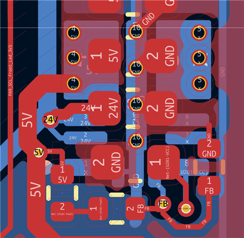
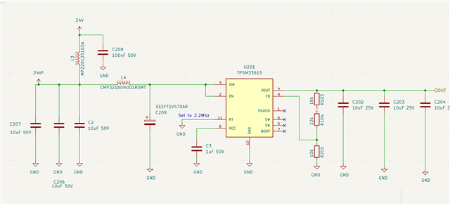
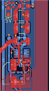
I have already build two versions of the board, the first one one without input PI filter (just 30uF X7R), the other one with the filter shown below. I think the layout is reasonable though, as always, it could be improved. 

I checked for regulation oscillations, load step responses with a 200MHz scope and they look all nice and clean. I read 

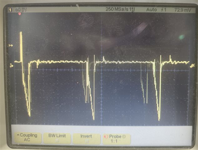
Power consumption is at 5V/40mA typically without any load spikes. The device stays cool. With this input filter, the ripple at the devices input is quite noticeable as can be seen in the screenshot.

I also tried to shorten the line to the 1uF Vcc cap. See below. Didn't help either.

Do you see any hint on why the devices fail? A quick response would be fine as we cannot reasonably test this design iteration due to this problem.


Input voltage With pi filter Vin=28V, Vout=5V, load 40mA.

Manual addition of a 2nd 1uF Cap at VCC with shorter lines.

  • As I hit send to early:
    I found this forum entry: TPSM33625: Device damage after 20s of operation
    which seems to be very related. That was the reason I impletemented the Electrolytic capacitor.
    Attached is also a picture of the device - maybe it helps to identifiy any possible counterfeits. Note that in this picture the device is shifted. However, the issue holds for devices which are properly mounted.

  • Hi Alex,

    The device requires at least 4.7uF of ceramic input capacitance placed close to the device pin. As the schematic shown has the ceramic before the input filter and none after, this is not recommended for this device. The input and output traces are also fairly thin, which adds extra impedance/inductance on these traces where are not recommended.

    The input voltage ripple does look large and may cause a voltage overstress condition on the device input, resulting in damage.

    If you are worried about a counterfeit possibility, please provide the lot info that your received these units with along with a picture of the label on the reel or box.

    Thank you,

    Joshua Austria

  • Hi Josuhua, 

    first, being an Austrian myself, I love being supported by Austria ;-)

    after 11 broken devices, we finally have one which seems to survive power-on without an inrush current limiter. As you suggested I added capacitors close to the supply line. I used 3uF instead of 4.7uF for the moment.

    To understand the criticality of a ceramic capacitor close to the supply I checked the routing of the first board we did. This had quite OK capacitor connection for the first of 3 10uF caps (see picture below) but also did not survive power-ons. Also a  few samples of this board showed failures after about 5-20min operation.

    This oscillogram shows the time of death of one device - it shorts the supply line after 3ms of 28V  power being applied. No spikes are noticeable here. Of course, the means of measurement were limited to an old 200Mhz scope with passive probes and around 20mm ground loop. Yet, I do not expect noticeable spikes due to the rather beefy Zener diode in parallel to the input pins anyway.


    I have now one specimen which works. It is one with the new layout with a PI filter with an electrolytic capacitor and a manually added 30V Zener and 3uF ceramic. One of the 3 1uF capacitors is very close to the supply pin with a short GND connection.

    Looking at the reference design in the eval module, I see how your design is very well optimized in terms of inductance and impedance. So my two design mistakes: having no damping capacitor in the first design and having no ceramic close to supply in the second design led to those issues. I am a bit worried that the design actually fails catastrophically when not being implemented quite carefully. My result is in contrast to what the datasheet says: 4.7uF is mandatory, 100nF optional, a PI Filter desirable since the first design had 30uF. Can you confirm that a design with PI filter, 4.7uF and 100nF is robust and does not need e.g. the use of the EN pin as suggested in other forum entries which talk about similar failures? In your experience do you see any other considerations to achieve a robust design which are often overlooked (apart from the obvious correct choices of correct values and power loss considerations)?

    Any input is welcome.

     Alex

  • Hi Alex,

    Having the 4.7uF close to the IC is mandatory for this device. It should also not be separated from the IC VIN pin with an inductor in between as this added impedance essentially makes it such that the 4.7uF ceramic is not seen by the IC. In addition TI suggests that the utilized capacitors are rated for at least 2x the voltages they are set to experience to avoid significant capacitance de-rating. 

    A Pi Filter is commonly used with buck converters to attenuate the conducted EMI noise that radiates from the operation of the buck converter. This allows them to pass a variety of conducted EMI standards. However, if not properly damped, excess parasitic impedances on the VIN trace will cause the input voltage to ring, getting worse when the circuit is loaded. Adding in the capacitors via the wires as shown in your photo is also not ideal as these wires carry extra impedances and parasitic inductances. Please read this application note for more details on the use case for a PI filter and the use of a damping electrolytic capacitor: https://www.ti.com/lit/an/snva489c/snva489c.pdf.

    In my experience, for an integrated inductor buck module, the most important components to keep close to the IC pins are those on the FB pin, VIN pin, and VCC pin. There is usually more leeway on the RT resistor, EN resistors, and the output capacitors. Here are the reasons why the aforementioned FB, VIN, and VCC connections are critical to remain close to the device:

    • The VIN capacitor is part of the high di/dt loop of the device and provides the supply for the high side switch. Extra impedance/inductance on this trace will affect the SW node and can further affect the regulation of the device. If you are using a high frequency input capacitor, it is best to keep this one in particular as close to the VIN and GND pins as possible to help with radiated EMI performance (as the high frequency band is the most susceptible to radiated noise for a buck converter).
    • The FB pin is where the device will sense the output voltage setpoint. It is important that the connections that are on this pin to have reduced impedance/inductance as to not harm the regulation of the device.
    • The VCC provides the voltage rail that the internal circuitry of the devices operates off of. Any degradation of this supply will result in worse/erratic behavior for the device overall.

    Hope this was able to clarify some of the reasonings behind these connections. More layout guidelines are available in the datasheet in section 8.5.1. Please let me know if you need any additional support,

    Joshua Austria