LM5143A-Q1: Technical Questions Regarding LM5143A-Q1 2-Phase / 4-Phase Synchronous Buck Operation

Part Number: LM5143A-Q1
Other Parts Discussed in Thread: LM5143-Q1

Tool/software:

I have several questions regarding the LM5143A-Q1 in our application:

  1. High-Side MOSFET Overheating
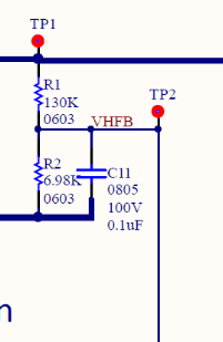
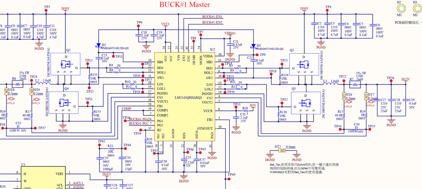
    We are using a two-phase synchronous buck converter with an input voltage of 25 V, output voltage of 15 V, and a load current of 23 A. The high-side MOSFET temperature (ISC0805NLSATMA1, gate resistor changed to 7.5 Ω) reaches 140 °C. What countermeasures can be implemented to further increase the output current to 35 A?


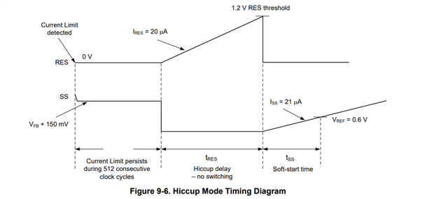
        2. Sawtooth Output Voltage & RES Pin Pulses
            If the output voltage exhibits a sawtooth switching waveform, the RES pin outputs pulses, and VDDA outputs 5 V, what could be the cause of this behavior? How can this abnormal condition be resolved?

        3. Determining Fault or Protection Mode

            How can we determine whether the LM5143A-Q1 is faulty or has entered a protection mode?

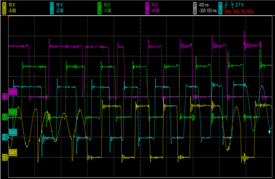
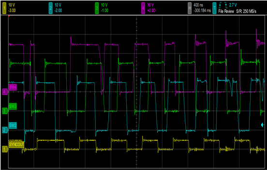
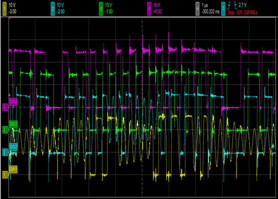
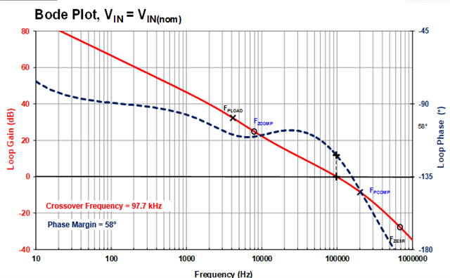
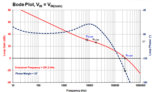
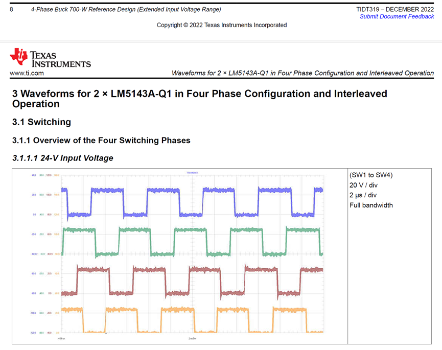
        4. 4-Phase Synchronization Issue

           We are using two LM5143A-Q1 devices to achieve a 4-phase synchronous buck configuration. Input voltage is 25 V, output voltage is 15 V, and there is no load. To verify the 4-phase synchronization, we measured CH1_SW1–PGND, CH2_SW2–PGND, CH3_SW3–PGND, and CH4_SW4–PGND. The CH4_SW4–PGND waveform does not match expectations (we expected SW3 to lead SW4). Measuring CH4_SYNCOUT (same as CH4 waveform) relative to SW1, SW2, and SW4 shows that the phases are not in the expected 90°, 180°, 270°, and 360° sequence. The ideal waveform should match the reference waveform in the TI documentation.

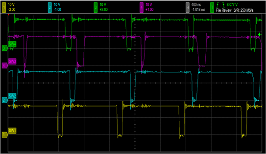
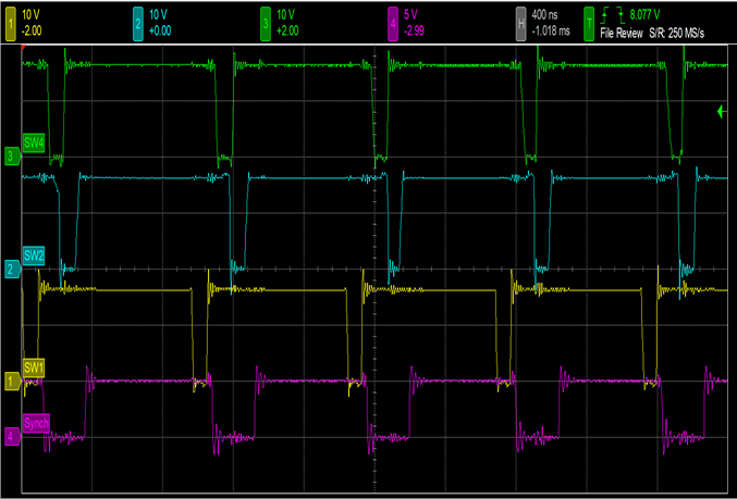
Could you please help us analyze these issues and suggest possible solutions?

Thank you for your support.

Best regards,

YUMING

  • Hello Yuming

    How is the behavior at lower load currents of 5-10A. Could you please share the SW waveforms at 5A current?

    If you're seeing pulses at the RES pin, this most likely indicates that the current limit protection is being triggered. This additional data point would help us understand if the issue persists across different load conditions or is specific to higher currents.

    Additionally, could you please share the filled QuickStart for your design? This would give me more complete information about your implementation

    Thank you

    Regards

    Onkar Bhakare

  • Hi Onkar:

      Apologies for the delayed response. The attached figure shows the SW-node waveforms at a 5 A load.

    Could you advise on the possible cause of the oscillation seen on SW1 and SW2?

    We also observe that SW1, SW2, SW3, and SW4 sometimes switch in order. Is this behavior expected?

    The following shows the current LM5143-Q1 Quickstart Design configuration for your reference.

    https://docs.google.com/spreadsheets/d/10v15ki_UtsdKey5BotfdEzC5Y4a5UaL6/edit?usp=sharing&ouid=104433332549816947365&rtpof=true&sd=true

    Thank you

    Regards

    YUMING

  • Hello YUMING

    It appears to be a instability, need to verify power stage component and compensation network. Could you please share direct Quickstart file itself, as we don't have google drive access.

    Meanwhile you can try increasing output caps and see if it helps

    Thank you

    Regards

    Onkar Bhakare

  • Hi Onkar:

        Apologies for the inconvenience. It appears that you were unable to open the document. The following shows the current LM5143-Q1 Quickstart Design configuration for your reference. We are not certain why the XLSM file could not be imported. Therefore, we have converted it into a PDF file for your reference. Could you please help us review and confirm?

    LM(2)5143-Q1 quickstart design.pdf

    Thank you

    Regards

    YUMING

  • Hello Yuming

    Stability margins looks fine as pet the QuickStart, 580 uF cap with 60% derating

    1. Whether all the caps are ceramic? or there are EL caps as well. I couldn't verify all the caps from schematic, I could see only 2x22uF at the output. Kindly share the part no. of EL cap, if it is used in design. Additionally, share the full schematic 
    2. Is full load current 70A or 35A?
    3. What is the status of DEMB, can you connect to VDDA and check
    4. Avoid resistor for bottom FET, it could lead to spurious turn ON, try shorting it to zero. Top FET resistor can be reduced below 5 ohm, if there is no excessive ringing at gate

    QuickStart file for reference - /cfs-file/__key/communityserver-discussions-components-files/196/1663.LM_2800_2_2900_5143_2D00_Q1-quickstart-design-tool-_2D00_-revB2.xlsm

  • Hi Yuming

    Do you have the similar FB configuration here for 4 phase design. Could you please remove 0.1uF cap at FB node and try. This cap will add a pole in to the loop and might lead to instability 

    Thank you

    Regards

    Onkar Bhakare

  • Hi Onkar:

       Thank you for your reply.Please see our reply below:

    1. Whether all the caps are ceramic? or there are EL caps as well. I couldn't verify all the caps from schematic, I could see only 2x22uF at the output. Kindly share the part no. of EL cap, if it is used in design. Additionally, share the full schematic 

    --> The ceramic capacitor model is GRM32ER71E226KE15L. Apologies for not providing the complete schematic earlier — please find the full circuit diagram below. In our two-phase synchronous buck converter testing, the output (Vout) was initially configured with eight 22 µF ceramic capacitors. When the load current exceeded 5 A, significant output voltage ripple was observed. To investigate, we added a 220 µF electrolytic capacitor, which improved the output voltage stability.   7127.BUCK CONVERTER.pdf

    2. Is full load current 70A or 35A?

    -->Our design target is a 4-phase synchronous buck converter with a 15 V output and a maximum load current of 70 A. Could you advise on the required amount of output capacitance to ensure stable operation?

    3. What is the status of DEMB, can you connect to VDDA and check

    -->VDDA has been measured at 5 V, and the primary LM5143A-Q1's DEMB pin is floating. Should the DEMB pin be connected to any signal?

    4. Avoid resistor for bottom FET, it could lead to spurious turn ON, try shorting it to zero. Top FET resistor can be reduced below 5 ohm, if there is no excessive ringing at gate

    -->Is this configuration appropriate, with 0 Ω gate resistors for both turn-on and turn-off on the bottom FET, and 7.5 Ω for turn-on and 0 Ω for turn-off on the top FET?

    5. Do you have the similar FB configuration here for 4 phase design. Could you please remove 0.1uF cap at FB node and try. This cap will add a pole in to the loop and might lead to instability 

    -->The VHFB pin is intended for input voltage sensing. We will remove the 0.1 µF capacitor connected to this pin and proceed with further testing.

    6. Could you please provide a simple explanation of the Bode plot shown above? Is it better when the dashed line is closer to the red line, or when the dashed line shows a smoother variation? We are mainly concerned with the system stability.

    Thank you

    Regards

    YUMING

  • Hello Yuming

    DEMB must be connected either to AGND or VDDA. Connect it to VDDA for FPWM mode, while DEM mode can be achieved by connecting it to AGND.

    For practical stability, we recommend keeping phase margin above 45 deg. However, to have sufficient margin 60 deg is recommended 

    I'm currently out of office, I'll get back to you on rest of the question in day or 2

  • Hi Onkar:

       Thank you for your reply. What would be the impact or possible behavior if the DEMB pin is left floating?

    Thank you

    Regards

    YUMING

  • Hi Onkar:

       Thank you for your reply. What would be the impact or possible behavior if the DEMB pin is left floating?

    Thank you

    Regards

    YUMING

  • Hi Yuming

    I'm not sure how device will react if it is left floating. It is not recommended to leave it open. Connect it to either VDDA or AGND.

    Regards

    Onkar Bhakare

  • Hi Onkar:

        I appreciate your response. We would appreciate your support in addressing the related questions raised on August 20.

    Thank you

    Regards

    YUMING

  • Hello Yuming,

    I appreciate your follow-up. I'll be back in the office on July 28th and will address your questions as soon as I return.

    Thank you

    Regards,

    Onkar Bhakare

  • Hello Yuming

    Here are my comments on unanswered question.

    Our design target is a 4-phase synchronous buck converter with a 15 V output and a maximum load current of 70 A. Could you advise on the required amount of output capacitance to ensure stable operation?

    Output cap used derates roughly 70 % at 15V output, giving only 53 uF cap at the output. 

    With current combination of output cap and compensation network converter is unstable

    I would suggest increasing cap to 12*22uF and using following compensation network for starting values. 

    Rc1 5.1 kOhm
    Cc1 3.3 nF
    Cc2 33 pF

    Bode plot with 12*22uF + above compensation network

    You might need to optimize the compensation network based on experimental bode plot and transient response. 

    Is this configuration appropriate, with 0 Ω gate resistors for both turn-on and turn-off on the bottom FET, and 7.5 Ω for turn-on and 0 Ω for turn-off on the top FET?

    If ringing is not severe at Top FET gate, resistance can reduce below 5 ohm. 4.7 ohm can be sed as starting value.

     Could you please provide a simple explanation of the Bode plot shown above? Is it better when the dashed line is closer to the red line, or when the dashed line shows a smoother variation? We are mainly concerned with the system stability.

    For practical stability phase margin of above 45 deg is considered good enough. However, to have sufficient margin from instability and critical damped response PM of 60 deg is recommend. 

    Hope this helps

    Thank you 

    Regards

    Onkar Bhakare


  • Hi Onkar:

     Thank you for your suggestion. Your recommendation has been effective.  This topic can be closed. Thank you.

    Thank you for your support.

    Best regards,

    YUMING

  • Hello Yuming

    Glad it helped. Kindly close the thread

    Thank you

    Regards

    Onkar Bhakare