Other Parts Discussed in Thread: PMP21683, , UCC256302, UCC256403
Tool/software:
Hello,
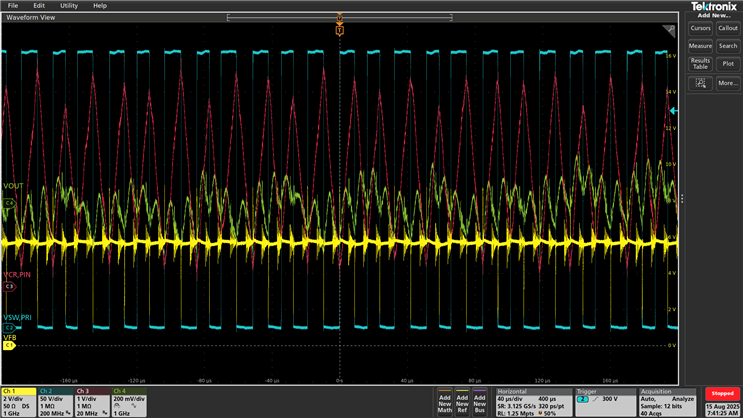
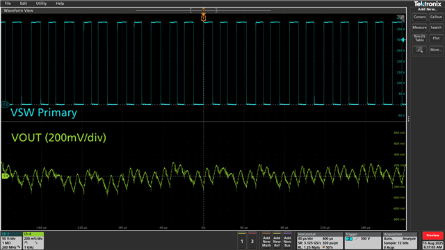
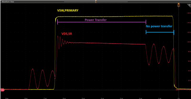
We are working with a redesigned version of the 550W EVM PMP21683, it has been updated to use the UCC256402 instead of the UCC256302. We are able to regulate 54Vout, but our objective with this EVM is to minimize frequency jitter, in order to more accurately analyze AC losses at a fixed frequency. However, we have not been able to minimize this jitter. Below is an example; the shown trace is a persistence plot of the primary Switch Node, where color brightness indicates the prevalence of the EVM operating at that condition:
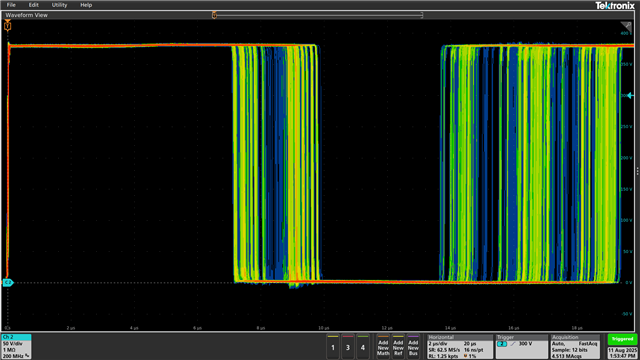
The above capture is taken at 540W (10A @ 54V) in steady-state, and we are seeing the switching frequency vary from 51.5kHz to 73.5kHz, with no clear operating point.
Is the UCC256402 designed to have this amount of frequency variation?
Also, the PMP21683 test report shows a typical switching frequency of about 83kHz at roughly the same load. With the same magnetics and resonant tank, why might we be operating at a lower switching frequency range compared to this design?
We have made adjustments to the VCR capacitor divider, but have encountered issues there also. When we used the pair of capacitors recommended by the design file, we saw even more jitter and this instability was even leading to OCP or another fault.
It was only when we decreased the VCR divider pair that we saw more consistent operation. Is this divider intended to be used to adjust the steady-state frequency variation?
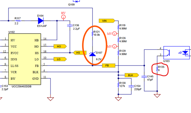
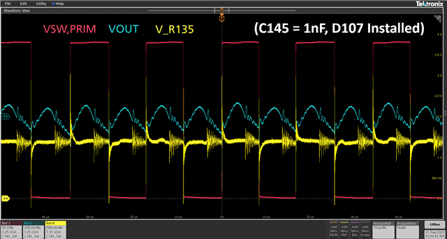
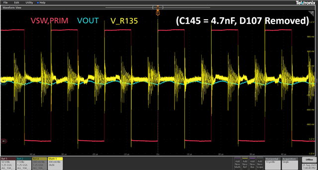
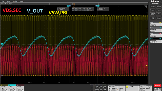
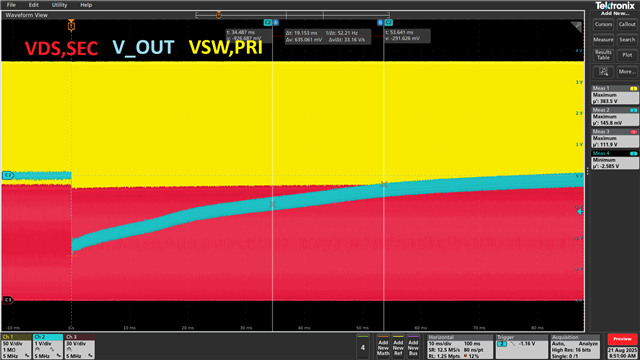
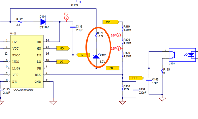
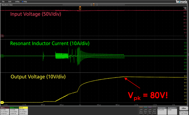
We have made other changes to try and prevent the frequency variation, as well. One change we initially made in moving from the UCC256402 to the UCC256302 was the removal of the pull-up diode on the FB pin (see D107 below). It was our understanding that this diode should be unnecessary for the UCC25640x series controller, because of the higher IFB current source used to bias the optocouple. However, removing this diode or insufficiently biasing it was leading to major instability, including at startup, where output voltage would reach more than 75V, before regulating back to 54V (see below before and after the diode was biased correctly).
What might cause this pull-up diode to be necessary?
Before:
After:

We also have questions about the "Compensation and Transient" design calculator provided by TI. We first attempted to choose values for the compensation network which provided a 4kHz crossover frequency and >35deg phase margin, but this led to a very slow transient response that we deemed unacceptable. After incrementing the RV/CV pole in the compensation network to give the best transient response, we plugged these values into the design calculator and they showed a -60 degree phase margin, even though the actual response was the best we'd seen.
Why might there be such a discrepancy?
Kind regards,
Orion Kress-Sanfilippo