LM3409: T_on too short on most pulses

Part Number: LM3409
Other Parts Discussed in Thread: TPS92640

Tool/software:

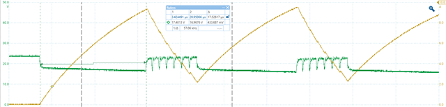
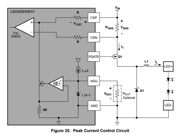
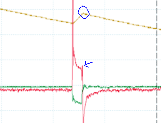
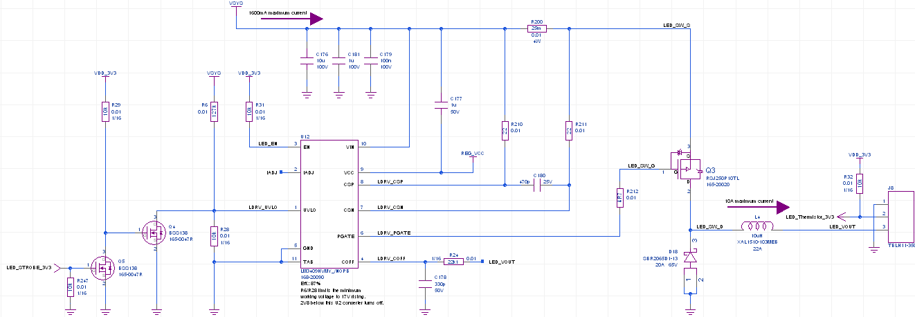
We successfully made designs with LM3409 before, but this one does not work as it should. As you can see below, most of the times when the P-FET is turned on (gate voltage seen in green) the LED current (shown in yellow) barely rises before the FET is turned off again. The time corresponds closely to the minimum on-time specified in the datasheet. I also posted the schematic we are using, the only difference to previous projects is, that we only drive a single LED, meaning V_IN is 24V while V_OUT is only 4V with maximum LED current of 10A. The oscilloscope screenshot is at V_ADJ of 1.24V.

/resized-image/__size/3530x1894/__key/communityserver-discussions-components-files/196/Pumbaa-LED-driver-full-power-evaluation-2025_2D00_08_2D00_19.png

/resized-image/__size/2644x916/__key/communityserver-discussions-components-files/196/Pumbaa-LED-driver-schematic.png

  • Hi Niklas,

    There could be a couple things going on here.

    1.) Your Toff network may not be sized correctly for the 10A output current at this low duty cycle. Note that most LM3409 designs use <5A output current. You can increase the Coff capacitor to 470pF, as this is the typically recommended value. If necessary, you can also increase the Roff resistor.

    2.) What is your desired LED current? According to the datasheet equations, for 25mΩ sense resistor with Viadj = 1.24V, your peak inductor current is set to 9.92A.

    You state the LED Vf is 4V at 10A, but the LED is not seeing 10A with these component values. What diode is used? What is the minimum Vf at the expected LED current? This may affect your duty cycle and min-on-time calculations.

    I do not see any capacitance at the output. Are you applying shunt-FET dimming to the LED?


    3.) Also keep in mind the minimum ripple requirement. For 25mΩ sense resistor, you require almost 1A of ripple. Increasing your Coff to 470pF will also increase your ripple.

    I recommend double checking your component values with the datasheet equations.

    4.) On your initial pulse, the peak current sense is triggered when the inductor current reaches 4.697 A which is less than half of your set point. Are you sure the Iadj voltage is set to 1.24V?

    I notice your re-circulating diode has a very high junction capacitance, especially at low reverse voltages. It is possible that when the PMOS is turned on, there is a large current spike charging the diode capacitance that triggers the peak current sense while bypassing the inductor current measurement. If you have a high voltage differential probe, you can take the differential voltage measurement directly across the sense resistor to determine if the peak current threshold is reached.

    If you require further support on this issue, please provide the following:

    Input/ output requirements and switching frequency

    Scope Capture:
    Inductor current (or Δ Rsense voltage)
    Switch node voltage
    COFF pin voltage
    Output voltage

    Thanks,

    Zach

  • Hi Zach,

    first of all, I want to thank you for the quick and thorough response.

    The purpose of this circuit is to drive a single LE D P0MQ with average currents from 0.5-8A set via the analog dimming function. I attached the sheet I used to calculate the parameters here: LM3409 calc sheet.xlsx . Let me know if you need additional information that is not provided here or in the schematic I attached in my previous image. The missing output capacitor is an oversight on my end, but we had a previous project work just fine without one.

    Addressing 4) : The 4.697A shown in the picture are the average current over one "cycle", the actual peak LED current is 8A. Measuring I_ADJ did give ~1.22V.

    Here are some of the additional measurements you requested:

    After writing my message yesterday, I checked what would happen if I connected four LEDs in series instead of just one, but saw no real change:

    We only have one differential probe rated for 24V, a HZ 109, and even though I used the shortest cables I could get away with, we see substantial voltage spikes:

    /resized-image/__size/3520x1886/__key/communityserver-discussions-components-files/196/Pumbaa-LED-driver-R_5F00_SNS-diff-probe-2025_2D00_08_2D00_20.png

    The voltage on the switching node on the other hand looks fine to me:

    /resized-image/__size/3526x1888/__key/communityserver-discussions-components-files/196/Pumbaa-LED-driver-SW_5F00_node-2025_2D00_08_2D00_20.png

    Same with the output voltage, if you ignore the spikes:

    /resized-image/__size/3528x1890/__key/communityserver-discussions-components-files/196/Pumbaa-LED-driver-output-voltage-2025_2D00_08_2D00_20.png

    The voltage at C_off however looks more interesting:

    /resized-image/__size/3530x1890/__key/communityserver-discussions-components-files/196/Pumbaa-LED-driver-C_5F00_off-voltage-2025_2D00_08_2D00_20.png

    Zooming out you can see that the only time we even come close to the correct voltage is when C_off is purposefully ignored by the IC, I assume as a feature to improve behaviour on the first pulse:

    /resized-image/__size/3526x1892/__key/communityserver-discussions-components-files/196/Pumbaa-LED-driver-C_5F00_off-voltage-multi_2D00_cycle-2025_2D00_08_2D00_20.png

    The biggest issue with the measurements is that the voltage spikes at the oscilloscope are masking a lot of what is going on when the P-FET switches. Unfortunately I couldn't use a spring contact and had to use wires, but even with keeping them as short as possible these screenshots were the best I could do on short notice.

    Please let me know what you recommend as our next steps. I can of course adjust C_off or R_off, but it would be nice to first have my calculations verified. I cannot switch out the diode (or any other large components like the FET or inductor) without destroying my board and the only place for an output cap I could find is at the LED directly, which puts 10cm (4") between that cap and the LED driver.

    Best regards,

    Niklas Meyer

  • Hi Niklas,

    Thanks for the additional measurements and information.

    I can see in your differential measurement that you are getting spikes over 1.6V. The peak current threshold is triggered at ~250mV. These voltage spikes are due to high inrush current that charges the very large capacitance of the diode and PFET. Normally there is a "blanking period" in which the threshold is not triggered due to short-duration inrush current. However, your differential Rsense voltage remains high due to inrush for longer than the minimum on time which is longer than the blanking period.

    Your PFET is rated to 100V and the diode 65V. This is way to high for this 24V application. Note that there is a relationship between the voltage rating and the capacitance. You will likely need to select smaller components that have a lower voltage rating and less capacitance. Essentially, the large capacitance is causing high inrush currents that are false triggering the peak current threshold on every cycle.

    Your PFET gate charge is also very high at 60 nC. There is some guidance in the datasheet on a method to reduce false triggering due to PFET input capacitance. However, even with this change I believe your diode capacitance would still cause the comparator to trigger.

    Your calculation sheet seems fine except that you chose a 25mΩ sense resistor instead of the 29mΩ resistor that was calculated.

    I also recommend including output capacitance on your next design revision. LM3409 does not "need" output capacitance to function, but based on your output voltage measurements it looks like it would help reduce your output ripple quite a bit. 

    Regards,

    Zach

  • Hi Zach,

    I see what you are saying about the transistor and diode being the wrong size for this application. Could you maybe quantify the blanking period you mentioned?

    I did the suggested modification to the bypass capacitor and while it did improve the situation somewhat (the pulses for T_on are now almost twice as long at 190ns), the current is still not regulated correctly.

    Afterwards I managed to replace the transistor with a DMP6180SK3-13, but this did not improve the switching behaviour at all. I ordered a new diode as well (RBR10BM40AFH) and will check next week if that can solve my problem. Let me know if you think I should try other components as well.

    Best regards,

    Niklas Meyer

  • Hi Niklas,

    I'm glad modifying the bypass capacitor helped somewhat... If you changed the FET after modifying this cap, I wouldn't expect much of a difference as the gate charge current is already being bypassed. However, this change could still improve your overall efficiency once we get the desired operation. 

    The blanking period is not specifically called out in the datasheet, but to start I would make sure the inrush current duration is less than the minimum on-time. I would really need to see another scope capture with the differential probe to tell what is happening during the new 190ns on-time.

    Keep me updated on the results with the new diode. This Schottky diode selected looks much more appropriate for this application.

    As for other components, I am still concerned about the 25mΩ sense vs the calculated 29mΩ. I am also curious if adjusting the differential filter across your sense resistor has any effect. You can compare your diff probe measurement with the capacitor removed vs different values of capacitance populated to see if there is a trend.

    Regards,

    Zach

  • Hi Zach,

    the new diodes are stuck in customs, but I managed to find an STPSL15L45CB to try out and did see some improvement, the P-FET is now on for ~370ns:

    /resized-image/__size/2860x480/__key/communityserver-discussions-components-files/196/Pumbaa-LED-driver-new-diode-2025_2D00_08_2D00_27.png

    I have to caution trusting the large spike on the differential measurement though, as its size changes every time I touch the measurement wires, so most of that is probably just EMI.

    Regarding the differential filter, all of the measurements I shared so far were without the capacitor, as I wanted to see if I was over-dampening the differential amplifier. I can try to increase the size to 1nF. Problem is I can only guesstimate the bandwidth of the regulator, do you have that information available?

    Best regards,

    Niklas Meyer

  • Hi Niklas,

    I'm glad to see the improvement, it looks like we are getting closer.

    The LM3409 does not have the typical closed-loop bandwidth like most switching converters. Instead it has a "feed-forward" control based on the controlled off-time. The differential filter should be designed to remove those noise spikes on your sense node which are triggering the internal comparator.

    From your scope capture, I can see the noise persists for the duration of your on-time effectively presenting as a large offset voltage that is close to the threshold. Then there is a small spike that puts the delta over the comparator threshold which triggers the off-time. Perhaps adjusting your differential filter can remove these spikes.

    Regards,

    Zach

  • Hi Zach,

    I got the new diodes, but there was no measurable difference to the STPSL15L45CB I tried before, so it seems like those were already "good enough". Furthermore I tried both 1nF and 4.7nF differential filter caps:

    1nF is reaching 520ns:

    /resized-image/__size/2858x1880/__key/communityserver-discussions-components-files/196/Pumbaa-LED-driver-1nF-filter-2025_2D00_08_2D00_27.png

    4.7nF is getting to ~680ns, where the switching behaviour seems almost normal:

    /resized-image/__size/3018x1878/__key/communityserver-discussions-components-files/196/Pumbaa-LED-driver-4n7-filter-DAC-at-250-2025_2D00_08_2D00_28.png

    However, I do see that the first few pulses are higher, before the system reaches a steady state at ~7A average current:

    /resized-image/__size/3530x1892/__key/communityserver-discussions-components-files/196/Pumbaa-LED-driver-4n7-filter-DAC-at-250-steady-state-2025_2D00_08_2D00_28.png

    While this could be acceptable, the problem is that at lower target currents, the system is too slow and does not dim the LED correctly (I need 1/20 analog dimming or better):

    /resized-image/__size/2992x1882/__key/communityserver-discussions-components-files/196/Pumbaa-LED-driver-4n7-filter-DAC-at-20-2025_2D00_08_2D00_28.png

    I also checked if with the new components I can connect the cap at VCC back to VIN, but immediately saw that the voltage spikes across the resistor are real enough to still be a problem:

    /resized-image/__size/3006x1882/__key/communityserver-discussions-components-files/196/Pumbaa-LED-driver-4n7-filter-DAC-at-250-VCC-cap-back-to-VIN-2025_2D00_08_2D00_28.png

    After this measurement I also got an improvement of my measurement setup and connected a 50MHz current probe between the sense resistor and the source-terminal of the FET. What is very surprising to me is that there are no spikes whatsoever visible on that measurement:

    /resized-image/__size/3022x1884/__key/communityserver-discussions-components-files/196/Pumbaa-LED-driver-4n7-filter-DAC-at-250-cap-normal-current-probe-on-source-2025_2D00_08_2D00_28.png

    At this point I feel like I am running out of options. The only thing I can still think of is doing permanent damage to my board: Remove the trace connecting I_adj and see if the voltage spikes are influencing the signal coming from the DAC. Is there anything else you recommend I should try first?

    Best regards,

    Niklas Meyer

  • Hi Niklas,

    Thanks for the detailed update.

    It looks like the increased differential filtering helped quite a bit. I am curious if this filter can be further optimized to improve the response.

    I'm not sure about the first few current pulses... I've heard that sometimes this can be caused by the current probe itself, something to do with the flux settling. I would also check your input voltage at the pin during these first pulses to make sure you have enough input cap to prevent the voltage from drooping too much.

    While this could be acceptable, the problem is that at lower target currents, the system is too slow and does not dim the LED correctly (I need 1/20 analog dimming or better):

    What is your IADJ voltage setting? The IADJ setting is not very accurate at low voltages, we typically recommend an IADJ voltage between 140mV and 1.24V. 1/20 analog dimming ratio is fairly high, could you use another dimming method such as PWM or shunt-FET?

    You are operating at a pretty low duty cycle at the high current setting. At the low current setting I assume your output voltage is significantly lower as well. You could try placing another LED in series to see if this helps at all.

    After this measurement I also got an improvement of my measurement setup and connected a 50MHz current probe between the sense resistor and the source-terminal of the FET. What is very surprising to me is that there are no spikes whatsoever visible on that measurement:

    These spikes are pretty fast for a 50MHz current probe, this is likely a bandwidth issue.

    You could also try placing your differential probe across the filter capacitor as this voltage is what the internal comparator actually sees. This should give you a better idea of how the device is responding.

    Regards,

    Zach

  • Hi Zach,

    first of all some background on my dimming requirements: The application requires analog dimming, PWM or shunt-FET methods are not suitable. For this LED my actual dimming requirements are 1/8-1/10, but this design is also supposed to work with a LZ4-00R608, which has higher forward voltage (~11.9V) but also much lower currents. That is where we got the 1/20 dimming requirement. However, at this point I think the best I will be able to achieve is have the same layout with different BoM-options for the two LEDs.

    Moving on to today's measurements:

    Without changing anything from my last test, I connected the differential probe across the filter cap as requested:

    /resized-image/__size/3006x1876/__key/communityserver-discussions-components-files/196/Pumbaa-LED-driver-4n7-filter-DAC-at-250-cap-normal-diff-probe-on-filter-2025_2D00_09_2D00_01.png

    The measured current spikes very quickly and the LED driver shuts down.

    I also tried to see if anything changes if I disconnect the I_adj pin and leave it floating:

    /resized-image/__size/3010x1880/__key/communityserver-discussions-components-files/196/Pumbaa-LED-driver-4n7-filter-cut-DAC-cap-normal-diff-probe-on-filter-2025_2D00_09_2D00_01.png

    With this change the current spikes even higher, even though what is most surprising to me is the first ramp, where the current does not reach 10A as it should and even more important the differential voltage seems to follow this very well. I would have expected to see a differential voltage of 1.24V/5 = 248mV before the gate is shut off. Actually, I never saw a voltage of 248mV without disconnecting the I_adj pin and even then just on some spikes that probably contain a good amount of measurement error due to EMI spikes.

    Best regards,

    Niklas Meyer

  • Hi Niklas,

    The switching behavior looks a lot different when you are probing across the filter capacitor. In this case I do believe that the measurement configuration is causing noise to couple into the comparator and change the performance of the circuit. I was hoping that this measurement would provide more insight but I see that is not the case, thanks for trying anyways.

    I think I understand your dimming requirements. I agree that using BOM variants is the best option to achieve a high-range, low-range design for different LEDs. The achievable dimming ratio with the iadj pin is about 1/8 or so for best accuracy, which should be in your desired range.

    Let me know if you have any more questions on this, and good luck with your design.

    Thanks,

    Zach

  • Hi Zach,

    what are there any next steps you would recommend? After swapping every connected component apart from the inductor without getting an improvement it feels like there is no lead on what I should improve for the next iteration of the design. Could there be something in the layout that might be causing these anomalies?

    If there is nothing else that might give an answer to this problem, it might make sense to look into alternative solutions. Are there any parts in TI's portfolio that might be better suited for my application? My own search on your website did not turn up anything promising apart from maybe the TPD92640.

    Best regards,

    Niklas Meyer

  • Hi Niklas,

    What improvement are you looking for? In your previous response, you said the performance pictured below would be acceptable and you will use a BOM variant for the lower range.

    Unfortunately, there are not many options for driving these high current levels. TPS92640 is also listed as 2-Ω 1A gate drive, although it looks like the typical resistances are a bit lower so the performance could be better. Of course, TPS92640 is also a synchronous converter which has other benefits such as efficiency, but will also have a slower ramp time because it has a control loop with compensation and output capacitance.

    You mentioned that you are not using PWM dimming but you must have some on/off timing requirements for the LEDs... can you clarify this? Can you provide more information about your application? What is the most important: efficiency, ramp-time, cost?

    I will need detailed information on your application and requirements in order to recommend the best solution.

    Another option is to parallel multiple channels to get higher currents. Two monolithic devices such as TPS92519 in parallel would get you to 8A and could save costs on the large FETs and Diodes required for a controller. You can refer to the app-note below for more information.

    https://www.ti.com/lit/an/sluaac0/sluaac0.pdf? 

    Regards,

    Zach

  • Hi Zach,

    I was hoping to get more than the roughly 1/8 of dimming factor that I achieved with the configuration of tying the VCC cap to CSN and increasing the differential filter to 4n7. While it is acceptable, it is just the bare minimum of what we need. Also, it feels kind of bad having to go to a non-standard connectivity scheme on this solution, if our previous designs did just fine without it.

    To describe our application in more detail, we have a pulsed projector with minimum on-time of 20us (to which we can add a 10-20us ramp-up time, the lower the better) and maximum on-time of 20ms. Due to the minimum on-time requirements we think that only analog dimming will work and the minimum required dimming factor is 1/8 for both LEDs, with one LED being designed for 8A peak current at ~4V (6A average, ~40% max duty-cycle over 1s) and the other for 2.5A at ~12V (2A average, ~20% max duty-cycle over 1s). Efficiency is the next most important factor, but the total cost of the driver solution should be below 5$ if possible.

    Best regards,

    Niklas Meyer

  • Hi Niklas,

    You may be able to get more than 1/8 analog dimming but the accuracy decreases at these higher dimming ratios. I'm not sure what previous designs you are comparing this to... what output current level was achieved with the previous designs?

    A minimum on-time of 20µs is very fast and would not be achievable with a standard control-loop device.

    It sounds like the LM3409 is the best available option for this application. Most new devices are synchronous, monolithic devices with limited current due to the integrated FETs. I often see designers looking to LM3409 for the fast hysteretic control and flexibility of sizing components for higher currents. Unfortunately, this device was not designed for applications greater than ~5A as the gate drive, dead time, and blanking period are not optimized for these high current levels.

    I don't have any more recommendations for the schematic besides experimenting a bit more with the differential filter to see if it can be further optimized.

    If you want to send me the layout I can take a look to see if any improvements can be made there.

    Regards,

    Zach

  • Hi Zach,

    I understand what you are saying on the lack of alternative parts, that does match my research.

    If you want to take a look at the layout, I cannot publicly share the design we were analyzing so far, but I made a test board with the recommended changes, that I would like your feedback on. I am hoping, that the compact switching node and tight switching loop will improve the situation.

    schematic_EPM2A - LM3409 LED driver Eval_variant_Full.pdf

    FAB.zip

    Best regards,

    Niklas Meyer

  • Hi Niklas,

    The layout looks pretty good, I only have a couple suggestions...

    First, you should remove the thermal reliefs from your input connections (VIN and GND) and use a direct connection. It looks like the rest of your power path uses direct connects which is good.

    I notice your PGATE trace width is ~8mil or less. Its not a long trace but increasing it to ~12mil could help reduce the inductance. It looks like you have plenty of room to widen this trace. I'm not sure if we addressed this previously, but we typically recommend to start with a 0-ohm gate resistor and increase the resistance if necessary.

    I would also consider how you want to manage the heat as this is a very small board with a lot of power. Do you plan to connect a heatsink to the bottom side? I can't tell from the Gerber files if you have thermal vias but I recommend placing some at the D1 and Q1 pads. Thermal vias in the ground pour around these component could also help.

    I understand you do not want to share the other design on the public forums. If you would like feedback for the other layout, feel free to send me the files directly and I can response over private chat. 

    Thanks,

    Zach

  • Hi Zach,

    I implemented your feedback and ordered the board, I will be receiving it in two weeks. I don't think it makes sense to look at the older layout as we will just implement this one if it works.

    For thermal management I bought some small heat-sinks you can glue on the transistor and the diode, together with a fan and limiting myself to short pulses I don't worry too much.

    I will let you know the results of my testing.

    Best regards,

    Niklas Meyer

  • Hi Zach,

    the new boards arrived and they work as intended. Seems like we had a major layout issue. Everything up to and including the dimming factor improved, I can get the blue LED down to ~600mA even with the increased differential filter capacitor.

    Thank you for your help on this journey to a working design.

    Best regards,

    Niklas Meyer