UCC29002: Improving current settling time and expected current waveform behavior

Part Number: UCC29002
Other Parts Discussed in Thread: INA293, INA187

Tool/software:

Hi Ulrich,
Regarding my previous question which is now locked, we've finally had time to do more testing on our system and upon doing more detailed testing we noticed some things that we think might be unusual.

1)The time for each of the individual channel's current to settle into steady state is very long, >50x the voltage settling time. Voltage settles in approximately 7ms but current of the individual channels settle roughly after 350ms regardless of the size of the current step change.
2)The current sharing stabilizes in what we think might be an unusual manner.   After the initial section that looks like an underdamped oscillation (approx the first 10ms or so), until the currents reach steady state it looks more like some sort of a piecewise function.
3)All this behavior is seen with 2,3, and 4 power supplies enabled
4)I should note we are using a low side current shunt with an INA293A2IDBVR between the shunt resistor and the CS+ inputs to improve handling of negative inputs beyond the -0.3V specified in the UCC29002 datasheet.

The attached image shows 3 of the 4 CSO lines (IMON0-2 in the image) and the 4th trace is the high side shunt prior to the electronic load (sum of all 4 supplies). While not shown, voltage stabilizes within 7ms of the initial rising edge and the 4th CSO line behaves similarly to the ones shown.  Please ignore the large amount of noise that can be seen on the CSO line traces as we've proven that that is a measurement artifact  

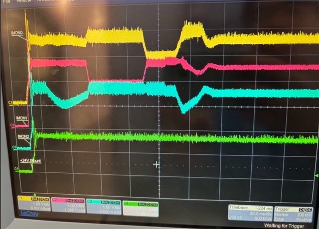
Is this all expected behavior?  Also how can we improve the response time to reach steady state?  My concern is that under heavy load, the duration of time where the currents are unbalanced is potentially long enough for one of my supplies to trip over current protection.

  • Hello B C, 

    I cannot address this issue in depth at this time.  I'll take it up again next Monday.

    However, the gross "piece-wise" variations over most of the 300ms of settling time are NOT expected inherent behavior of the UCC29002 controller, but must be instigated by some external influence (maybe noise on the LS inputs of each device?) of the current control. 

    It is expected that the current response time should be slower than the voltage loop by at least 10~20 times.  
    This involves accurately determining the power modules' V-loop 0dB cross-over frequency (fco_mod) and setting the EAO response to at least 1/10 of that fco_mod. 
    Please ensure that this was done. 

    Notwithstanding the previous comments, the UCC29002 is designed to start up by aggressively driving high adjustment to the module output voltages to get the currents up as soon as possible, then they settle out to equilibrium from there. 
    An alternate version of the IC UCC29002-1 has the aggressive start-up disabled and the EAO starts from 0V and gradually increases, so the sharing gradually increases to equilibrium.  It may take a bit longer than the aggressive manner, but should be more smooth and calm. 
    However, this difference does not account for the behavior seen in the screenshot, in my estimation.  I think something else is going on there. 
    But maybe you can try the UCC29002-1 to see if it helps to avoid it. 

    Regards,
    Ulrich

  • Hi Ulrich,
    I made a mistake, we're already using the UCC29002-1.  We previously tried the UCC29002 and it did not work at all with our power module as the Adj pin current would be permanently stuck sinking 6mA. Swapping to the UCC29002-1 immediately made things operate.

    We did determine the power module's db crossover frequency and we've set the EAO response below 1/10th of that, even taking into account capacitor and resistor tolerances.  I've confirmed the calculations are compliant with TI's spreadsheet.  We did find an issue where we were not compliant with Vrshunt < ΔVadjMax/10.  Correcting this did not change the behavior though.

    I've also checked the LS inputs of each device and they're clean.   The LS line behaves in a similar piecewise manner and pretty much tracks the behavior of the CSO lines.

    After more experimentation, I've discovered that the piecewise variations only appear if the system goes below a minimum load current. In this case I've found it's about 1A.  If I go below 1A the next change in current shows these piecewise variations.  Even a small jump from 0A to 1A causes these piecewise variations.  However if I stay  above 1A, even jumps upto 18A produce essentially a square step on CSO and LS lines.   Any other thoughts on how to correct this or push the minimum load current lower to avoid this issue?  I've tried changing the current amplifier gain from 5 to 10 (along with any other required components for EAO compensation) and there was no change in minimum load current.

    Thanks,

    Bernard

  • Hi Bernard, 

    I checked the INA293 specs and found this bit of information: 

    It is possible that at the light load of <1A, the 4 modules might "juggle" current such that some negative current flows into one or more of the modules and the INA's take some time to sort out and settle to a steady-state, depending on how much negative they might have be subjected to.  

    If your modules are capable of accepting some negative current, this might be the root cause of the behavior. 
    You may need to consider output blocking diodes to prevent reverse current if this situation cannot be tolerated. 

    Please investigate and see if this might be the cause.

    Regards,
    Ulrich

  • Hi Ulrich,

    With how our pcb has been designed, testing with blocking diodes would either need to be done with great difficulty or require a new board spin so it's not something we want to do at the moment.  We're also investigating whether we can live with the 1a minimum load requirement.   In the meantime though, I was wondering if you think it would work to use the INA187A1 (or something similar) and tie the reference to gnd instead?  The INA187 datasheet does not mention overload recovery time for unidirectional measurements.

    Thanks

  • Hi Bernard, 

    Although your latest suggestion of using INA187A1 sounds like it should take care of the negative current issue, I am not familiar with the INA product line and can't offer adequate support for their use and limitations.  I recommend that you post a separate E2E thread for help with recovery times and other help, with "INA187" in the title so that it is routed to the correct group.  

    Meanwhile, assuming the INA187 device solves the negative current handling issue at <1A loading, please be sure that this device does not force the CS+ and CS- inputs to below -0.3V during this condition.  I expect that if the INA187 has only a positive bias voltage it should be unable to drive its output below GND, but it pays to verify and make sure.     

    Regards,
    Ulrich

  • Hi Ulrich,

    Ok I'll open up a new thread about the INA187A1.  I will make sure to verify that the CS+ and CS- inputs are not forced below -0.3V in that configuration.

    However, as a sanity check, I removed the external shunt amplifier and wired the shunt resistor terminals to match figure 7-2 in datasheet Rev J for high voltage low side current sensing.  I originally had the INA293A2IDBVR followed by a voltage divider as the input to CS+. This has been changed to the equivalent resistance as seen by the CS+ pin in order to maintain the same gain and keep all other components the same.  With this configuration, the piecewise waveforms are still being generated when starting with currents below 2A.   Also, at low currents I think there's always going to be the possibilty of backdriving a supply simply because of power supply output tolerances, +/-2.5% in my case (Radj has already been selected to cover this range).  I could trim them to be closer together as an experiment but not for production.  Any other suggestions to try?

    Thanks

  • Hi Bernard, 

    I think it is worth doing the experiment to trim the 4 modules' output voltages closer together to see if the onset of piecewise current toggling is pushed further below 1A load.  I agree it is not suitable for production, but it will lend insight into the source of the problem.   

    The only other suggestion I have is to expand the range of Radj to cover increase of Vout up to 6~7%, so that presumably the one module at +2.5% will get no adjustment and the one module at -2.5% will get almost full adjustment plus any additional adjustment to overcome distribution drops. 
    This presupposes that you may not have provided enough adjustment range with your Radj value.  

    On the other hand, if that doesn't improve anything, try the other way and reduce Radj to see if that has any beneficial effect.  

    Regards,
    Ulrich

  • Hi Ulrich,
    So we've tried all sorts of things to experiment
    -Swapping to the IN187A1 had no change in minimum load.  I asked about this IC in another thread and they mentioned it would still have an overload recovery as well if used with a single supply.
    -Trimming supplies closer together had no change in minimum load
    -Trimming the supplies further apart had no change either.  Interestingly though, even if 3 supplies were trimmed down to the minimum and one supply trimmed to the maximum, one of the trimmed down supplies almost always matches the CSO waveform of the trimmed up channel.  It was not always the same trimmed down channel that matched the trimmed up one.
    -We already had Radj set to 6-7% to cover the needed range.   When we reduced that, there was no change in minimum load either.
    -removing our external shunt amplifier (shunt resistor adjusted so none of the other components needed adjustment) had no change in minimum load either

    What did help was boosting the CS+ input voltage by reducing the voltage divider that followed the INA293A1 by about 30%.  This reduced the minimum load to 0.4A.  When load sharing only two supplies the min load was only 0.05A but with 4 supplies the min load was upto 0.4A.

    Now by reducing this voltage divider, I am now slightly below the Vrshunt< ΔVADJ(max)/10 limit in the design calculator.  Is it possible to go above this limit as my Acsa gain is fairly low? Or should I boost my Acsa gain further?

    Also, is it possible to DM you the design?  Perhaps it might help us look for some other things to try.

    Thanks